


关于Avago MGA-231T6 GPS低噪音(LNA)放大方案
出处:tyw 发布于:2011-07-30 17:49:25
Avago(发音为a-va’-go) Technologies拥有5,500多种系列产品,主要应用于无线和有线通信、工业、汽车、消费电子及存储和计算机等广阔的应用领域和终端市场。它在光电耦合器、红外线收发器、光通信器件、打印机ASIC、光学鼠标传感器和运动控制编码器等领域据称一直保持市场前3名的领导地位。Avago的产品通过代理商网络和直销队伍销售给40,000多家客户。
Avago 公司的MGA-231T6 是(0.9-3.5)GHz GPS//ISM/WiMAX低噪音放大器">低噪音放大器(LNA),采用GaAs 增强模式pHEMT工艺,具有高增益。低噪音和高线性特性,工作定压可低至1.8V,主要用作GPS, WLAN 和WIMAX低噪音放大器。本文介绍了MGA-231T6主要特性, 演示板,应用电路和所用元件表以及S参数测量参考平面。
Avago Technologies’ MGA-231T6 is a low-noise amplifier (LNA) designed for GPS/ISM/Wimax applications in the (0.9-3.5)GHz frequency range. The LNA uses Avago Tech-nologies’ proprietary GaAs Enhancement-mode pHEMT process to achieve high gain with very low noise figure and high linearity. Noise figure distribution is very tightly controlled. A CMOS-compatible shutdown pin is included either for turning the LNA on/off or for current adjust-ment.
The low noise figure and high gain, coupled with low cur-rent consumption make it suitable for use in critical low-power GPS applications or during low-battery situations.
MGA-231T6主要特性:
Very Low Noise Figure
High Gain and Linearity
Low External Component Count
Low Shutdown Current
CMOS compatible shutdown pin (SD) current @ Vsd= 1.8V : 0.11mA
Useable down to 1.8V supply
Adjustable current via single external resistor/voltage
Small package dimension: 2.0(L)x1.3(W)x0.4(H) mm Specifications (Typical performance @ 25°C) At 1.575GHz
Vdd = 2.85V, Vsd = 1.8V, Idd =4mA
– Gain = 17.1 dB
– NF = 1.06 dB
– Input IP3 = 0.2 dBm
– Input P1dB = 7.7 dBm
MGA-231T6应用:
LNA for GPS, WLAN and WIMAX

图1.MGA-231T6演示板和应用电路元件表
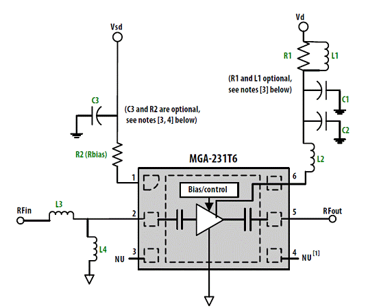
Notes:
1. Pin 4 must be left unconnected
2. L3 and L4 form the input matching network. C2 and L2 form a matching network at the output of the LNA.
3. L1 and R1 isolates the demoboard from external disturbances during measurement. It is not needed in actual application. Likewise, C1 and C3 mitigate the effect of external noise pickup on the Vdd and SD lines respectively. These components are not required in actual operation.
4. Bias control is achieved by either varying the SD voltage with/without R2, or fixing the SD voltage to Vdd and adjusting R2 for the desired current. R2 = 8.2 kOhm will result in 4mA when Vdd = 2.85V, Vsd = 1.8V or Vdd = 1.8V, Vsd = 2.6V. R2 = 5.6 kOhm will result in 6mA when Vdd = Vsd = 2.7V.
图2.MGA-231T6演示板和应用电路图
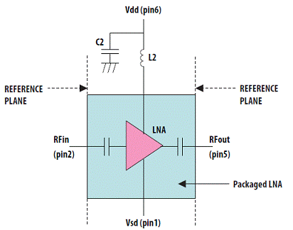
图3.MGA-231T6 S参数测量参考平面
详情请见:
https://www.avagotech.com/docs/AV02-2212EN
版权与免责声明
凡本网注明“出处:维库电子市场网”的所有作品,版权均属于维库电子市场网,转载请必须注明维库电子市场网,https://www.dzsc.com,违反者本网将追究相关法律责任。
本网转载并注明自其它出处的作品,目的在于传递更多信息,并不代表本网赞同其观点或证实其内容的真实性,不承担此类作品侵权行为的直接责任及连带责任。其他媒体、网站或个人从本网转载时,必须保留本网注明的作品出处,并自负版权等法律责任。
如涉及作品内容、版权等问题,请在作品发表之日起一周内与本网联系,否则视为放弃相关权利。
相关技术资料
- 模数转换 – 性能标准2024/4/8 16:37:02
- 解析 PWM (DAC) 性能:第 4 部分 – 非均匀占空比组2024/3/28 17:23:37
- 了解运算放大器的输出信号摆幅2024/3/18 16:29:20
- 模拟和数字传感器和转换器2024/3/7 16:39:16
- Microchip - 多通道优先级放大器的设计与应用2024/3/5 15:07:03
技术分类
广告

热门技术资料


