2N5638
2N5638
N-Channel Switch
鈥?This device is designed for low level analog switchng, sample and hold
circuits and chopper stabilized amplifiers.
鈥?Sourced from process 51.
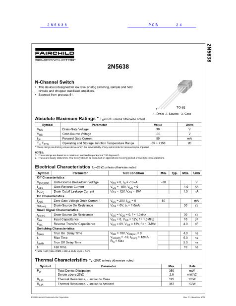
1
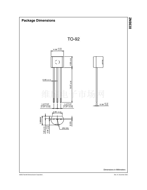
TO-92
1. Drain 2. Source 3. Gate
Absolute Maximum Ratings *
T
C
=25掳C unless otherwise noted
Symbol
V
DG
V
GS
I
GF
T
J
, T
STG
Drain-Gate Voltage
Gate-Source Voltage
Forward Gate Current
Operating and Storage Junction Temperature Range
Parameter
Value
30
-30
50
-55 ~ +150
Units
V
V
mA
掳C
* These ratings are limiting values above which the serviceability of any semiconductor device may be impaired.
NOTES:
1. These ratings are based on a maximum junction temperature of 150 degrees C.
2. These are steady state limits. The factory should be consulted on applications involving pulsed or low duty cycle operations.
Electrical Characteristics
T
C
=25掳C unless otherwise noted
Symbol
Off Characteristics
V
(BR)GSS
I
GSS
I
D(off)
I
DSS
r
DS(on)
r
ds(on)
C
iss
C
rss
t
d(on)
t
r
t
d(off)
t
f
Parameter
Test Condition
V
DS
= 0, I
G
= -10碌A
V
GS
= -15V, V
DS
= 0
V
DS
= 12V, V
GS
= 15V
V
DS
= 20V, I
GS
= 0
V
GS
= 0V, I
D
= 1.0mA
V
DS
= V
GS
= 0, f = 1.0kHz
V
DS
= 0, V
GS
= 12V, f = 1.0MHz
V
DS
= 0V, V
GS
= 12V, f = 1.0MHz
V
DD
= 10V, V
GS(on)
= 0
V
GS(off)
= -12, I
D(on)
= 12mA
R
G
= 50鈩?/div>
50
30
30
10
4.0
4.0
5.0
5.0
10
Min.
-30
-1.0
1.0
Typ.
Max.
Units
V
nA
nA
mA
鈩?/div>
鈩?/div>
pF
pF
ns
ns
ns
ns
Gate-Source Breakdown Voltage
Gate Reverse Current
Drain Cutoff Leakage Current
Zero-Gate Voltage Drain Current *
Drain-Source On Resistance
Drain-Source On Resistance
Input Capacitance
Reverse Transfer Capacitance
Trun On Delay Time
Rise Time
Trun Off Delay Time
Fall Time
On Characteristics
Small Signal Characteristics
Switching Characteristics
* Pulse Test: Pulse Width
鈮?/div>
300碌s, Duty Cycle
鈮?/div>
1.0%
Thermal Characteristics
T
A
=25掳C unless otherwise noted
Symbol
P
D
R
胃JC
R
胃JA
Parameter
Total Device Dissipation
Derate above 25掳C
Thermal Resistance, Junction to Case
Thermal Resistance, Junction to Ambient
Max.
350
2.8
125
357
Units
mW
mW/掳C
掳C/W
掳C/W
漏2002 Fairchild Semiconductor Corporation
Rev. A1, November 2002
2N5638相关型号PDF文件下载
-
型号
版本
描述
厂商
下载
-
英文版
TRANSISTOR | BJT | NPN | 60V V(BR)CEO | 100MA I(C) | TO-29
ETC
-
英文版
TRANSISTOR | BJT | NPN | 60V V(BR)CEO | 100MA I(C) | TO-29
-
英文版
TRANSISTOR | BJT | PNP | 50V V(BR)CEO | 5A I(C) | TO-3
ETC
-
英文版
TRANSISTOR | BJT | PNP | 50V V(BR)CEO | 5A I(C) | TO-3
-
英文版
Bipolar PNP Device in a Hermetically sealed TO66 Metal Packa...
SEME-LAB
-
英文版
Silicon NPN Power Transistors
ISC [Incha...
-
英文版
Silicon NPN Power Transistors
SAVANTIC [...
-
英文版
Bipolar PNP Device in a Hermetically sealed TO66 Metal Packa...
SEME-LAB [...
-
英文版
Bipolar PNP Device in a Hermetically sealed TO66 Metal Packa...
SEME-LAB
-
英文版
Silicon PNP Power Transistors
ISC [Incha...
-
英文版
Silicon PNP Power Transistors
SAVANTIC [...
-
英文版
Bipolar PNP Device in a Hermetically sealed TO66 Metal Packa...
SEME-LAB [...
-
英文版
TRANSISTOR | BJT | NPN | 80V V(BR)CEO | 2A I(C) | TO-66
ETC
-
英文版
Bipolar NPN Device in a Hermetically sealed TO66 Metal Packa...
SEME-LAB
-
英文版
Silicon NPN Power Transistors
ISC [Incha...
-
英文版
Silicon NPN Power Transistors
SAVANTIC [...
-
英文版
Bipolar NPN Device in a Hermetically sealed TO66 Metal Packa...
SEME-LAB [...
-
英文版
Bipolar PNP Device in a Hermetically sealed TO66 Metal Packa...
SEME-LAB
-
英文版
Silicon PNP Power Transistors
ISC [Incha...
-
英文版
Silicon PNP Power Transistors
SAVANTIC [...


 1
1
 2
2
 3
3
