鈻?/div>
Absolute Maximum Ratings
T
a
=
25掳C
Parameter
Collector-base voltage (Emitter open)
Collector-emitter voltage (Base open)
Emitter-base voltage (Collector open)
Collector current
Collector power dissipation
*
Junction temperature
Storage temperature
Symbol
V
CBO
V
CEO
V
EBO
I
C
P
C
T
j
T
stg
Rating
15
10
2
80
300
150
鈭?5
to
+150
Unit
V
V
V
mA
mW
掳C
掳C
1.1
+0.2
鈥?.1
1.1
+0.3
鈥?.1
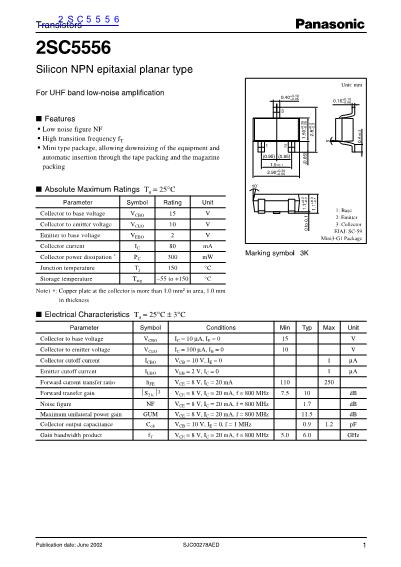
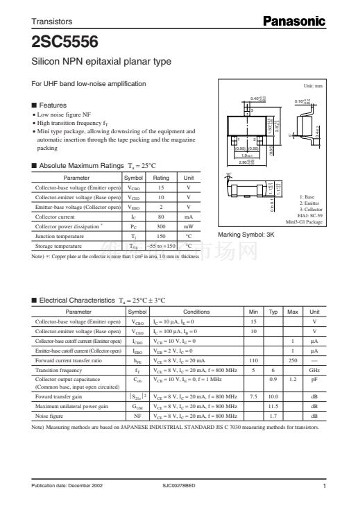
1: Base
2: Emitter
3: Collector
EIAJ: SC-59
Mini3-G1 Package
Marking Symbol: 3K
Note) *: Copper plate at the collector is more than 1 cm
2
in area, 1.0 mm in thickness
鈻?/div>
Electrical Characteristics
T
a
=
25掳C
卤
3掳C
Parameter
Collector-base voltage (Emitter open)
Collector-emitter voltage (Base open)
Collector-base cutoff current (Emitter open)
Emitter-base cutoff current (Collector open)
Forward current transfer ratio
Transition frequency
Collector output capacitance
(Common base, input open circuited)
Foward transfer gain
Maximum unilateral power gain
Noise figure
Symbol
V
CBO
V
CEO
I
CBO
I
EBO
h
FE
f
T
C
ob
铮
21e
铮?/div>
2
G
UM
NF
Conditions
I
C
=
10
碌A,
I
E
=
0
I
C
=
100
碌A,
I
B
=
0
V
CB
=
10 V, I
E
=
0
V
EB
=
2 V, I
C
=
0
V
CE
=
8 V, I
C
=
20 mA
V
CE
=
8 V, I
C
=
20 mA, f
=
800 MHz
V
CB
=
10 V, I
E
=
0, f
=
1 MHz
V
CE
=
8 V, I
C
=
20 mA, f
=
800 MHz
V
CE
=
8 V, I
C
=
20 mA, f
=
800 MHz
V
CE
=
8 V, I
C
=
20 mA, f
=
800 MHz
7.5
110
5
6
0.9
10.0
11.5
1.7
1.2
Min
15
10
1
1
250
Typ
Max
Unit
V
V
碌A
碌A
铮?/div>
GHz
pF
dB
dB
dB
Note) Measuring methods are based on JAPANESE INDUSTRIAL STANDARD JIS C 7030 measuring methods for transistors.
0 to 0.1
0.4
卤0.2
5藲
Publication date: December 2002
SJC00278BED
1


 1
1
 2
2
 3
3
