2SK3262-01MR
N-CHANNEL SILICON POWER MOS-FET
Features
High speed switching
Low on-resistance
No secondary breadown
Low driving power
Avalanche-proof
FUJI POWER MOS-FET
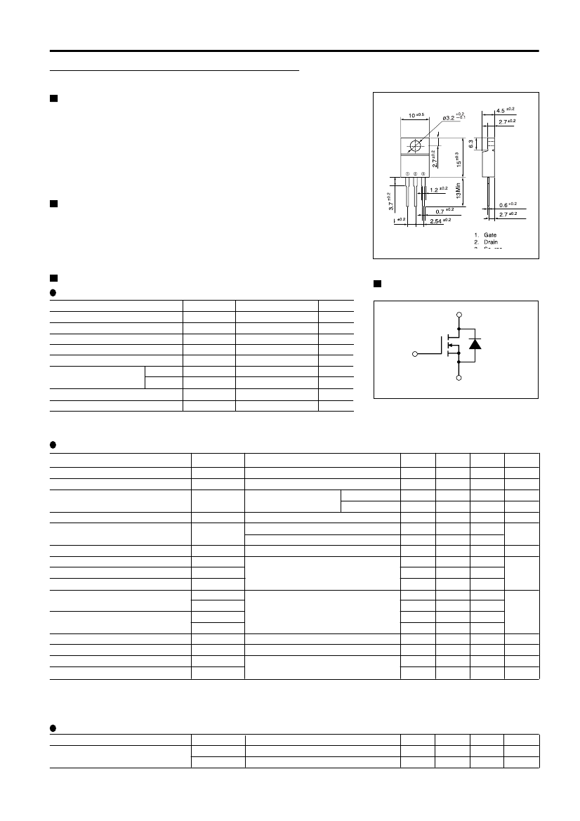
TO-220F15
Applications
Switching regulators
UPS (Uninterruptible Power Supply)
DC-DC converters
3. Source
2.54
Maximum ratings and characteristic
Absolute maximum ratings
(Tc=25掳C unless otherwise specified)
Item
Symbol
Drain-source voltage
V
DS
Continuous drain current
I
D
Pulsed drain current
I
D(puls]
Gate-source voltage
V
GS
Maximum Avalanche Energy
E
AV *1
Max. power dissipation Ta=25掳C P
D
Tc=25掳C P
D
Operating and storage
T
ch
temperature range
T
stg
Rating
200
卤20
卤80
卤20
355
2
45
+150
-55 to +150
Unit
V
A
A
V
mJ
W
W
掳C
掳C
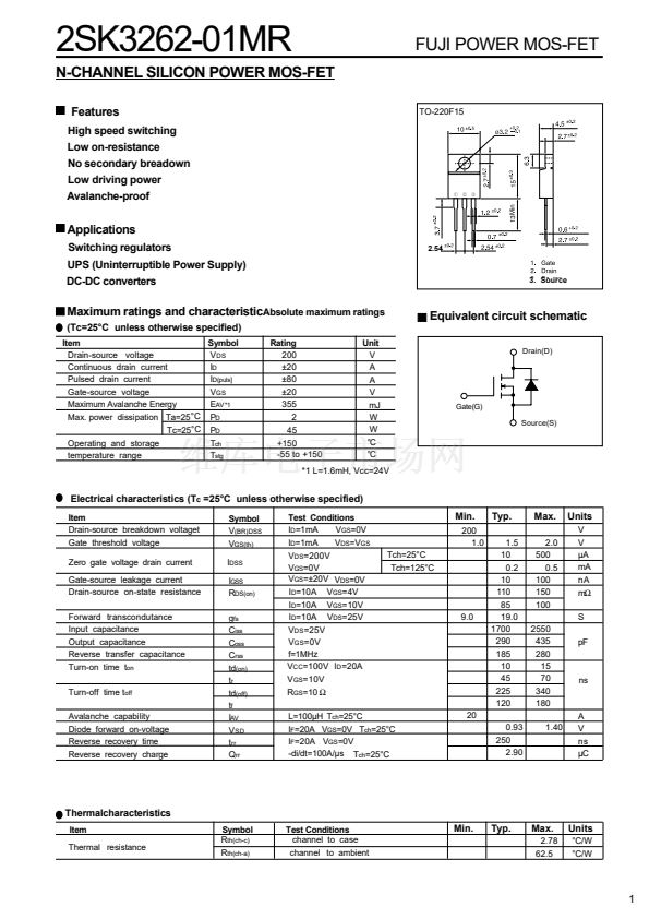
Equivalent circuit schematic
Drain(D)
Gate(G)
Source(S)
*1 L=1.6mH, Vcc=24V
Electrical characteristics (T
c
=25掳C unless otherwise specified)
Item
Drain-source breakdown voltaget
Gate threshold voltage
Zero gate voltage drain current
Gate-source leakage current
Drain-source on-state resistance
Forward transcondutance
Input capacitance
Output capacitance
Reverse transfer capacitance
Turn-on time t
on
Turn-off time t
off
Avalanche capability
Diode forward on-voltage
Reverse recovery time
Reverse recovery charge
Symbol
V
(BR)DSS
V
GS(th)
I
DSS
I
GSS
R
DS(on)
g
fs
C
iss
C
oss
C
rss
td
(on)
t
r
td
(off)
t
f
I
AV
V
SD
t
rr
Q
rr
Test Conditions
I
D
=1mA
V
GS
=0V
I
D
=1mA
V
DS
=V
GS
V
DS
=200V
V
GS
=0V
V
GS
=卤20V V
DS
=0V
I
D
=10A V
GS
=4V
I
D
=10A V
GS
=10V
I
D
=10A V
DS
=25V
V
DS
=25V
V
GS
=0V
f=1MHz
V
CC
=100V I
D
=20A
V
GS
=10V
R
GS
=10
鈩?/div>
L=100碌H T
ch
=25掳C
I
F
=20A V
GS
=0V T
ch
=25掳C
I
F
=20A V
GS
=0V
-di/dt=100A/碌s T
ch
=25掳C
20
0.93
250
2.90
1.40
Min.
200
1.0
Tch=25掳C
Tch=125掳C
Typ.
1.5
10
0.2
10
110
85
19.0
1700
290
185
10
45
225
120
Max.
2.0
500
0.5
100
150
100
2550
435
280
15
70
340
180
Units
V
V
碌A
mA
nA
m鈩?/div>
S
pF
9.0
ns
A
V
ns
碌C
Thermalcharacteristics
Item
Thermal resistance
Symbol
R
th(ch-c)
R
th(ch-a)
Test Conditions
channel to case
channel to ambient
Min.
Typ.
Max.
2.78
62.5
Units
掳C/W
掳C/W
1


 1
1
 2
2
 3
3
 4
4
