2SK3526-01L,S,SJ
FUJI POWER MOSFET
N-CHANNEL SILICON POWER MOSFET
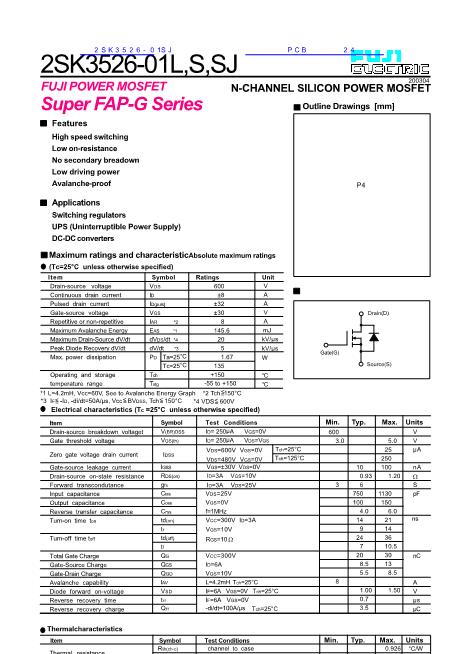
Outline Drawings [mm]
200304
Super FAP-G Series
Features
High speed switching
Low on-resistance
No secondary breadown
Low driving power
Avalanche-proof
P4
Applications
Switching regulators
UPS (Uninterruptible Power Supply)
DC-DC converters
Maximum ratings and characteristic
Absolute maximum ratings
(Tc=25掳C unless otherwise specified)
Ratings
600
卤8
卤32
卤30
8
145.6
20
5
1.67
135
Operating and storage
+150
-55 to +150
temperature range
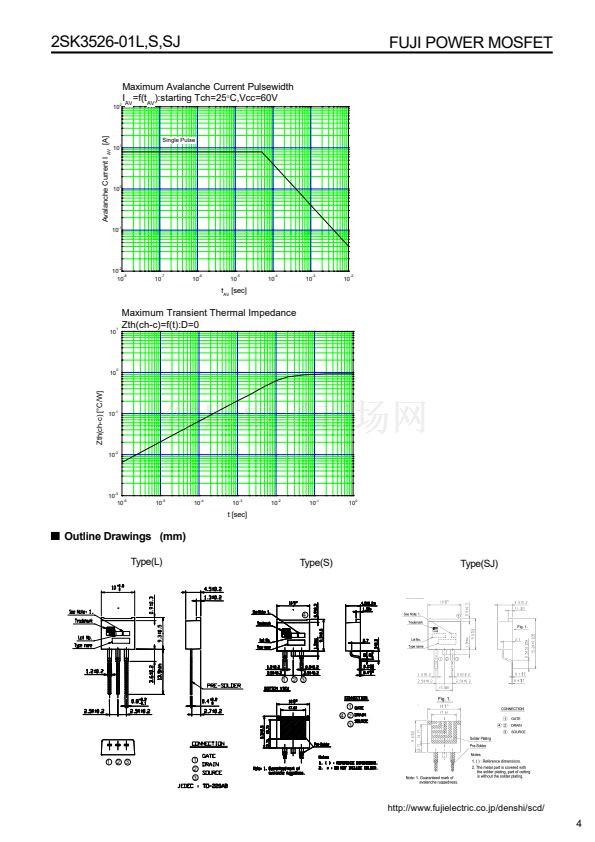
*1 L=4.2mH, Vcc=60V, See to Avalanche Energy Graph *2 Tch <150掳C
=
*3 I
F
< -I
D
, -di/dt=50A/碌s, Vcc < BV
DSS
, Tch < 150掳C
*4 VDS < 600V
=
=
=
=
Item
Drain-source voltage
Continuous drain current
Pulsed drain current
Gate-source voltage
Repetitive or non-repetitive
Maximum Avalanche Energy
Maximum Drain-Source dV/dt
Peak Diode Recovery dV/dt
Max. power dissipation
Symbol
V
DS
I
D
I
D(puls]
V
GS
I
AR
*2
E
AS
*1
dV
DS
/dt
*4
dV/dt
*3
P
D
Ta=25掳C
Tc=25掳C
T
ch
T
stg
Unit
V
A
A
V
A
mJ
kV/碌s
kV/碌s
W
掳C
掳C
Drain(D)
Gate(G)
Source(S)
Electrical characteristics (T
c
=25掳C unless otherwise specified)
Item
Drain-source breakdown voltaget
Gate threshold voltage
Zero gate voltage drain current
Gate-source leakage current
Drain-source on-state resistance
Forward transcondutance
Input capacitance
Output capacitance
Reverse transfer capacitance
Turn-on time t
on
Turn-off time t
off
Total Gate Charge
Gate-Source Charge
Gate-Drain Charge
Avalanche capability
Diode forward on-voltage
Reverse recovery time
Reverse recovery charge
Symbol
V
(BR)DSS
V
GS(th)
I
DSS
I
GSS
R
DS(on)
g
fs
C
iss
C
oss
C
rss
td
(on)
t
r
td
(off)
t
f
Q
G
Q
GS
Q
GD
I
AV
V
SD
t
rr
Q
rr
Test Conditions
I
D
= 250碌A
V
GS
=0V
I
D
= 250碌A
V
DS
=V
GS
V
DS
=600V V
GS
=0V
V
DS
=480V V
GS
=0V
V
GS
=卤30V V
DS
=0V
I
D
=3A V
GS
=10V
I
D
=3A V
DS
=25V
V
DS
=25V
V
GS
=0V
f=1MHz
V
CC
=300V I
D
=3A
V
GS
=10V
R
GS
=10
鈩?/div>
V
CC
=300V
I
D
=6A
V
GS
=10V
L=4.2mH T
ch
=25掳C
I
F
=6A V
GS
=0V T
ch
=25掳C
I
F
=6A V
GS
=0V
-di/dt=100A/碌s T
ch
=25掳C
T
ch
=25掳C
T
ch
=125掳C
10
0.93
6
750
100
4.0
14
9
24
7
20
8.5
5.5
1.00
0.7
3.5
Min.
600
3.0
Typ.
Max.
5.0
25
250
100
1.20
1130
150
6.0
21
14
36
10.5
30
13
8.5
1.50
Units
V
V
碌A
nA
鈩?/div>
S
pF
3
ns
nC
8
A
V
碌s
碌C
Thermalcharacteristics
Item
Thermal resistance
Symbol
R
th(ch-c)
R
th(ch-a)
Test Conditions
channel to case
channel to ambient
Min.
Typ.
Max.
0.926
75.0
Units
掳C/W
掳C/W
1


 1
1
 2
2
 3
3
 4
4
