鈩?/div>
......................卤250 ppm/掳C
above 2.2 M鈩?.................卤250 ppm/掳C
TCR Tracking .........................50 ppm/掳C
maximum; equal values
Resistor Tolerance ................See circuits
Operating Temperature
.................................-55 掳C to +125 掳C
Insulation Resistance
..................10,000 megohms minimum
Dielectric Withstanding Voltage
.............................................200 VRMS
Lead Solderability
.....Meet requirements of MIL-STD-202
Method 208
Environmental Characteristics
TESTS PER MIL-STD-202.........鈭哛 MAX.
Short Time Overload..................卤0.25 %
Load Life ....................................卤1.00 %
Moisture Resistance ..................卤0.50 %
Resistance to Soldering Heat
................................................卤0.25 %
Terminal Strength.......................卤0.25 %
Thermal Shock...........................卤0.25 %
Physical Characteristics
Flammability .........Conforms to UL94V-0
Lead Frame Material
..........................Copper, solder coated
Body Material ..................Novolac epoxy
How To Order
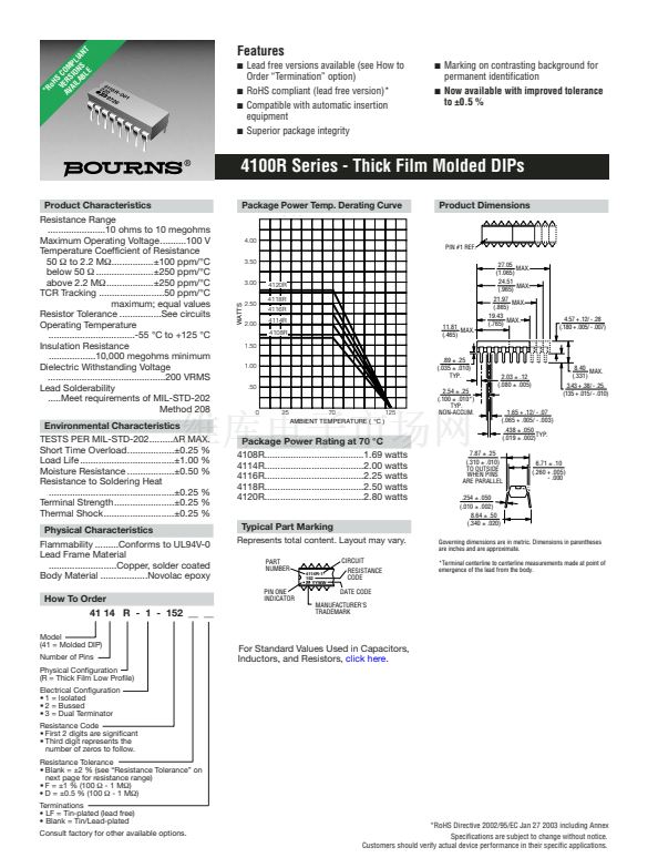
Package Power Temp. Derating Curve
G CU
4.00
Product Dimensions
PIN #1 REF.
3.50
3.00
2.50
2.00
1.50
1.00
.50
4120R
4118R
4116R
4114R
4108R
11.81
MAX.
(.465)
27.05
MAX.
(1.065)
24.51
MAX.
(.965)
21.97
MAX.
(.865)
19.43
MAX.
(.765)
WATTS
4.57 + .12/ - .28
(.180 + .005/ - .007)
.89
卤
.25
(.035
卤
.010)
TYP.
0
25
70
125
AMBIENT TEMPERATURE (
掳
C )
2.54
卤
.25
(.100
卤
.010*)
TYP.
NON-ACCUM.
2.03
卤
.12
(.080
卤
.005)
8.40
MAX.
(.331)
3.43 + .38/ - .25.
(135 + .015/ - .010)
1.65 + .12/ - .07
(.065 + .005/ - .003)
.438
卤
.050
TYP.
(.019
卤
.002)
Package Power Rating at 70
掳C
4108R......................................1.69 watts
4114R......................................2.00 watts
4116R......................................2.25 watts
4118R......................................2.50 watts
4120R......................................2.80 watts
Typical Part Marking
Represents total content. Layout may vary.
PART
NUMBER
4114R-1-
152
YYWW
7.87
卤
.25
(.310
卤
.010)
TO OUTSIDE
WHEN PINS
ARE PARALLEL
.254
卤
.050
(.010
卤
.002)
8.64
卤
.50
(.340
卤
.020)
6.71
卤
.10
(.260 + .005)
(.260
- .000)
Governing dimensions are in metric. Dimensions in parentheses
are inches and are approximate.
*Terminal centerline to centerline measurements made at point of
emergence of the lead from the body.
CIRCUIT
RESISTANCE
CODE
DATE CODE
PIN ONE
INDICATOR
41 14 R - 1 - 152 __ __
Model
(41 = Molded DIP)
Number of Pins
Physical Configuration
(R = Thick Film Low Profile)
Electrical Configuration
鈥?1 = Isolated
鈥?2 = Bussed
鈥?3 = Dual Terminator
Resistance Code
鈥?First 2 digits are significant
鈥?Third digit represents the
number of zeros to follow.
Resistance Tolerance
鈥?Blank = 卤2 % (see 鈥淩esistance Tolerance鈥?on
next page for resistance range)
鈥?F = 卤1 % (100
鈩?/div>
- 1 M鈩?
鈥?D = 卤0.5 % (100
鈩?/div>
- 1 M鈩?
Terminations
鈥?LF = Tin-plated (lead free)
鈥?Blank = Tin/Lead-plated
Consult factory for other available options.
MANUFACTURER'S
TRADEMARK
For Standard Values Used in Capacitors,
Inductors, and Resistors,
click here.
*RoHS Directive 2002/95/EC Jan 27 2003 including Annex
Specifications are subject to change without notice.
Customers should verify actual device performance in their specific applications.


 1
1
 2
2
