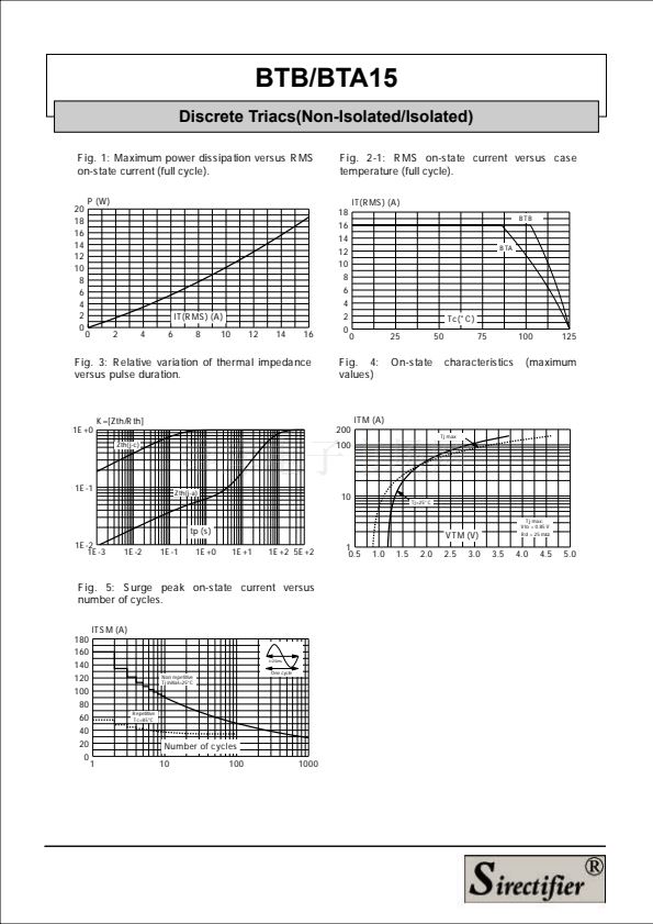
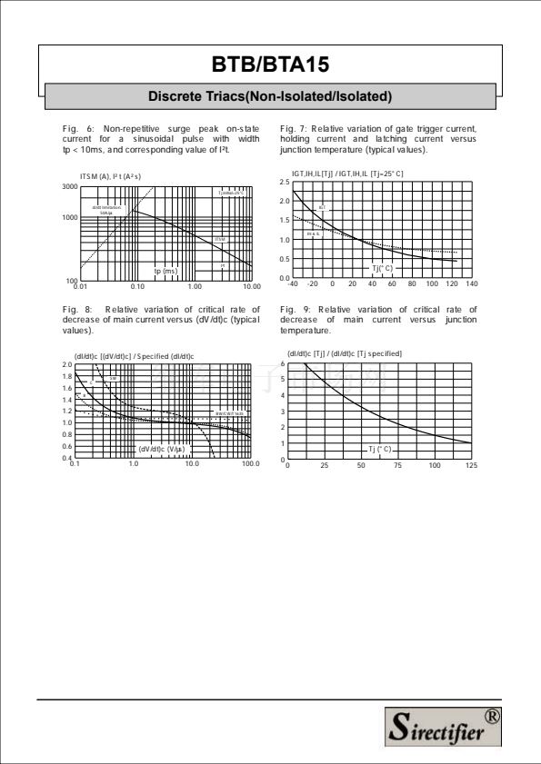
BTB/BTA15
Discrete Triacs(Non-Isolated/Isolated)
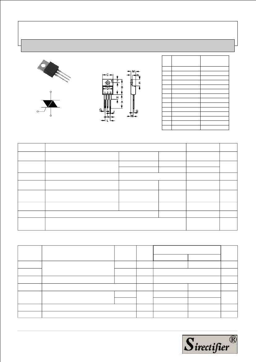
Dimensions TO-220AB
Dim.
A
B
C
D
E
F
G
H
J
K
M
N
Q
R
Inches
Min.
Max.
0.500 0.550
0.580 0.630
0.390 0.420
0.139 0.161
0.230 0.270
0.100 0.125
0.045 0.065
0.110 0.230
0.025 0.040
0.100
BSC
0.170 0.190
0.045 0.055
0.014 0.022
0.090 0.110
Milimeter
Min.
Max.
12.70 13.97
14.73 16.00
9.91 10.66
3.54
4.08
5.85
6.85
2.54
3.18
1.15
1.65
2.79
5.84
0.64
1.01
2.54
BSC
4.32
4.82
1.14
1.39
0.35
0.56
2.29
2.79
G
T2
T1
T2
G
T1
ABSOLUTE MAXIMUM RATINGS
Symbol
I
T(RMS)
I
TSM
I
虏
t
dI/dt
Parameter
RMS on-state current (full sine wave)
Non repetitive surge peak on-state
current (full cycle, Tj initial = 25掳C)
I
虏
t Value for
fusing
Critical rate of rise of on-state current
_
I
G
= 2 x
I
GT
, tr < 100 ns
TO-220AB
F = 60 Hz
F = 50 Hz
Tc = 100掳C
t = 16.7 ms
t = 20 ms
Value
15
168
160
144
Tj = 125掳C
50
Unit
A
A
A
虏
s
A/碌s
tp = 10 ms
F = 120 Hz
V
DSM
/V
RSM
Non repetitive surge peak off-state
voltage
I
GM
P
G(AV)
T
stg
T
j
Peak gate current
Average gate p ower diss ipation
Storage junction temperature range
Operating junction temperature
range
tp = 10 ms
tp = 20 碌s
Tj = 25掳C
Tj = 125掳C
Tj = 125掳C
V
DRM
/V
RRM
+ 100
V
A
W
掳C
4
1
- 40 to + 150
- 40 to + 125
ELECTRICAL CHARACTERISTICS (Tj = 25掳C, unless otherwise specified)
s
SNUBBERLESS鈩?and LOGIC LEVEL(3 Quadrants)
Symbol
Test Conditions
Quadrant
CW
I
GT
(1)
V
GT
V
GD
I
H
(2)
I
L
dV/dt (2)
V
D
= 12 V
V
D
= V
DRM
I
T
= 500 mA
I
G
= 1.2 I
GT
V
D
= 67 % V
DRM
gate open Tj = 125掳C
Tj = 125掳C
I - III
II
MIN.
MIN.
(dI/dt)c (2) Without snubber
R
L
= 33
鈩?/div>
R
L
= 3.3 k
鈩?/div>
Tj = 125掳C
I - II - III
I - II - III
I - II - III
MAX.
MAX.
MIN.
MAX.
MAX.
35
50
60
500
8.5
35
1.3
0.2
50
70
80
1000
14
V/碌s
A/ms
BTA/BTB
BW
50
mA
V
V
mA
mA
Unit


 1
1
 2
2
 3
3
 4
4
