鈥?/div>
鈥?Typical active current: 12.5 mA @ f = f
max
Low standby current
Automatic power-down when deselected
TTL-compatible inputs and outputs
Easy memory expansion with CE and OE features
CMOS for optimum speed/power
an automatic power-down feature that reduces power con-
sumption by more than 99% when deselected.
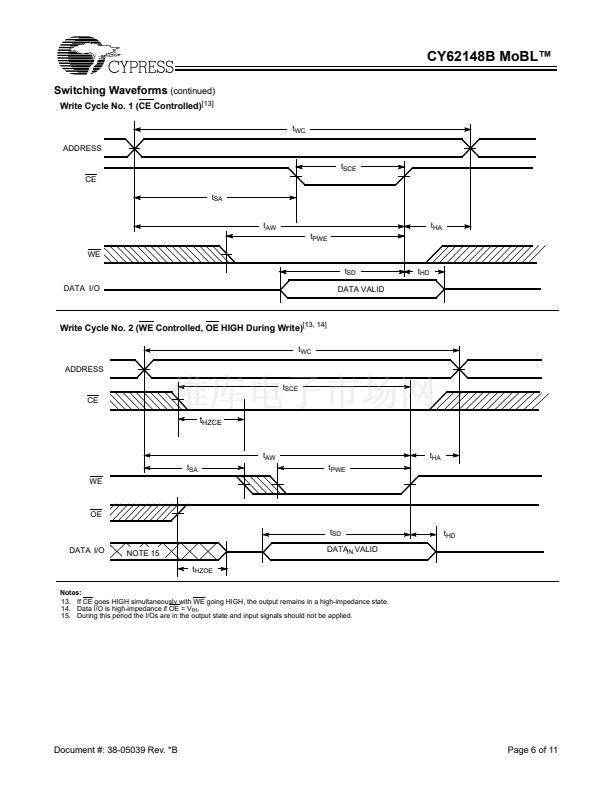
Writing to the device is accomplished by taking Chip Enable
(CE) and Write Enable (WE) inputs LOW. Data on the eight I/O
pins (I/O
0
through I/O
7
) is then written into the location speci-
fied on the address pins (A
0
through A
18
).
Reading from the device is accomplished by taking Chip En-
able (CE) and Output Enable (OE) LOW while forcing Write
Enable (WE) HIGH for read. Under these conditions, the con-
tents of the memory location specified by the address pins will
appear on the I/O pins.
The eight input/output pins (I/O
0
through I/O
7
) are placed in a
high-impedance state when the device is deselected (CE
HIGH), the outputs are disabled (OE HIGH), or during a write
operation (CE LOW, and WE LOW).
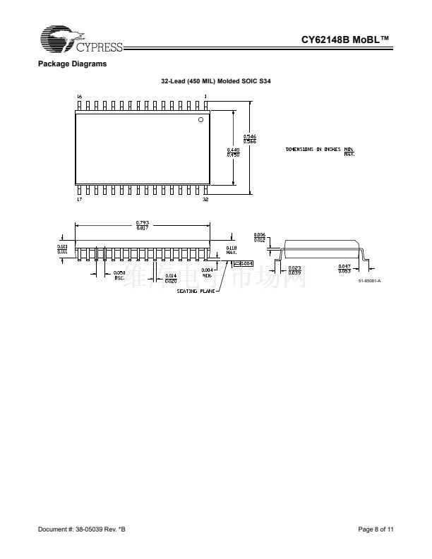
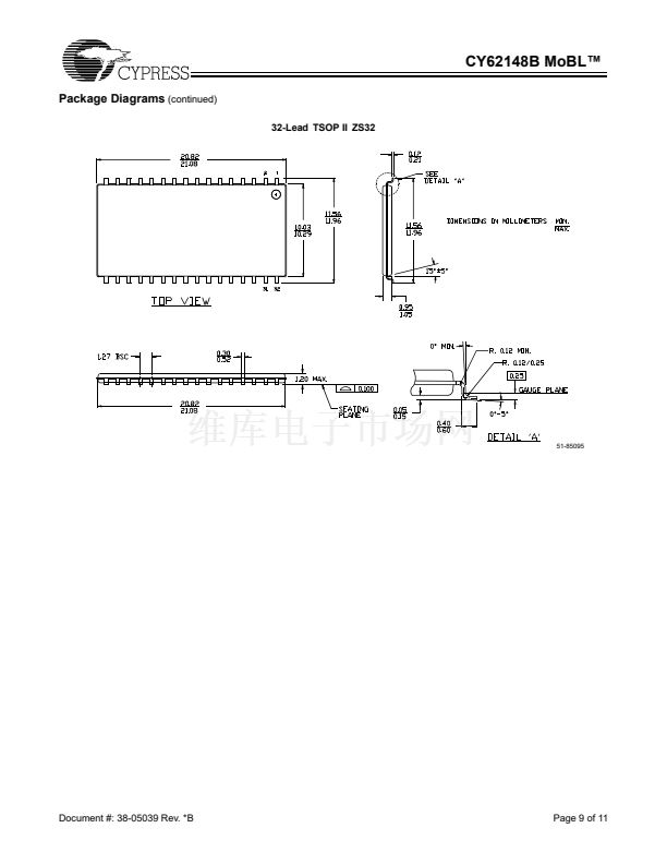
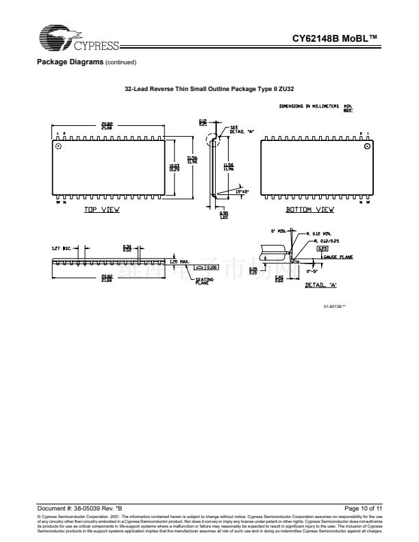
The CY62148B is available in a standard 32-pin 450-mil-wide
body width SOIC, 32-pin TSOP II, and 32-pin Reverse TSOP
II packages.
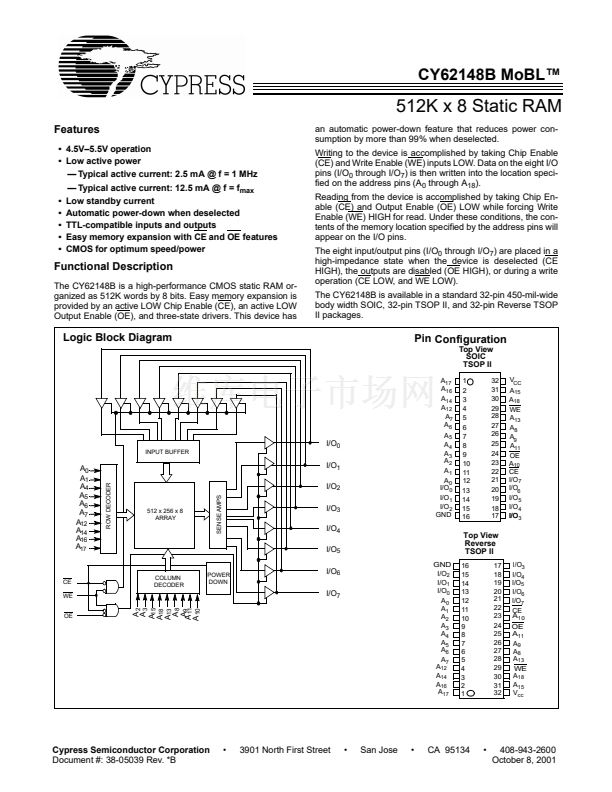
Functional Description
The CY62148B is a high-performance CMOS static RAM or-
ganized as 512K words by 8 bits. Easy memory expansion is
provided by an active LOW Chip Enable (CE), an active LOW
Output Enable (OE), and three-state drivers. This device has
Logic Block Diagram
Pin Configuration
Top View
SOIC
TSOP II
A
17
A
16
A
14
A
12
A
7
A
6
A
5
A
4
A
3
A
2
A
1
A
0
I/O
0
I/O
1
I/O
2
GND
1
2
3
4
5
6
7
8
9
10
11
12
13
14
15
16
32
31
30
29
28
27
26
25
24
23
22
21
20
19
18
17
V
CC
A
15
A
18
WE
A
13
A
8
A
9
A
11
OE
A
10
CE
I/O
7
I/O
6
I/O
5
I/O
4
I/O
3
I/O
0
INPUT BUFFER
A
0
A
1
A
4
A
5
A
6
A
7
A
12
A
14
A
16
A
17
I/O
1
ROW DECODER
I/O
2
SENSE AMPS
512 x 256 x 8
ARRAY
I/O
3
I/O
4
I/O
5
Top View
Reverse
TSOP II
GND
I/O
2
I/O
1
I/O
0
A
0
A
1
A
2
A
3
A
4
A
5
A
6
A
7
A
12
A
14
A
16
A
17
16
15
14
13
12
11
10
9
8
7
6
5
4
3
2
1
17
18
19
20
21
22
23
24
25
26
27
28
29
30
31
32
I/O
3
I/O
4
I/O
5
I/O
6
I/O
7
CE
A
10
OE
A
11
A
9
A
8
A
13
WE
A
18
A
15
V
cc
CE
WE
OE
COLUMN
DECODER
POWER
DOWN
I/O
6
I/O
7
Cypress Semiconductor Corporation
Document #: 38-05039 Rev. *B
A
2
A
3
A
15
A
18
A
13
A
8
A
9
A
11
A
10
鈥?/div>
3901 North First Street
鈥?/div>
San Jose
鈥?/div>
CA 95134
鈥?/div>
408-943-2600
October 8, 2001


 1
1
 2
2
 3
3
 4
4
 5
5
 6
6
 7
7
 8
8
 9
9
 10
10
 11
11
