1CY 626 4
PRELIMINARY
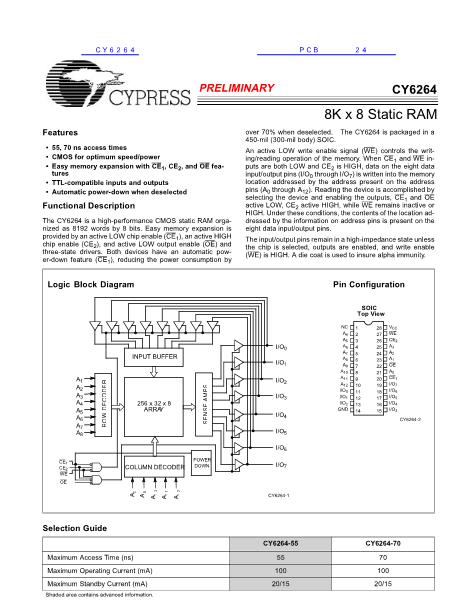
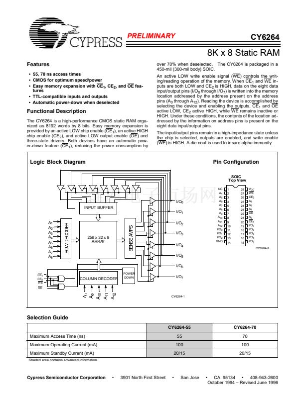
CY6264
8K x 8 Static RAM
Features
鈥?55, 70 ns access times
鈥?CMOS for optimum speed/power
鈥?Easy memory expansion with CE
1
, CE
2
, and OE fea-
tures
鈥?TTL-compatible inputs and outputs
鈥?Automatic power-down when deselected
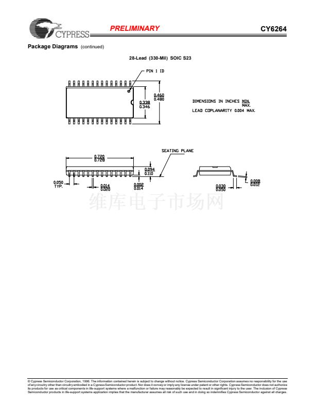
over 70% when deselected. The CY6264 is packaged in a
450-mil (300-mil body) SOIC.
An active LOW write enable signal (WE) controls the writ-
ing/reading operation of the memory. When CE
1
and WE in-
puts are both LOW and CE
2
is HIGH, data on the eight data
input/output pins (I/O
0
through I/O
7
) is written into the memory
location addressed by the address present on the address
pins (A
0
through A
12
). Reading the device is accomplished by
selecting the device and enabling the outputs, CE
1
and OE
active LOW, CE
2
active HIGH, while WE remains inactive or
HIGH. Under these conditions, the contents of the location ad-
dressed by the information on address pins is present on the
eight data input/output pins.
The input/output pins remain in a high-impedance state unless
the chip is selected, outputs are enabled, and write enable
(WE) is HIGH. A die coat is used to insure alpha immunity.
Functional Description
The CY6264 is a high-performance CMOS static RAM orga-
nized as 8192 words by 8 bits. Easy memory expansion is
provided by an active LOW chip enable (CE
1
), an active HIGH
chip enable (CE
2
), and active LOW output enable (OE) and
three-state drivers. Both devices have an automatic pow-
er-down feature (CE
1
), reducing the power consumption by
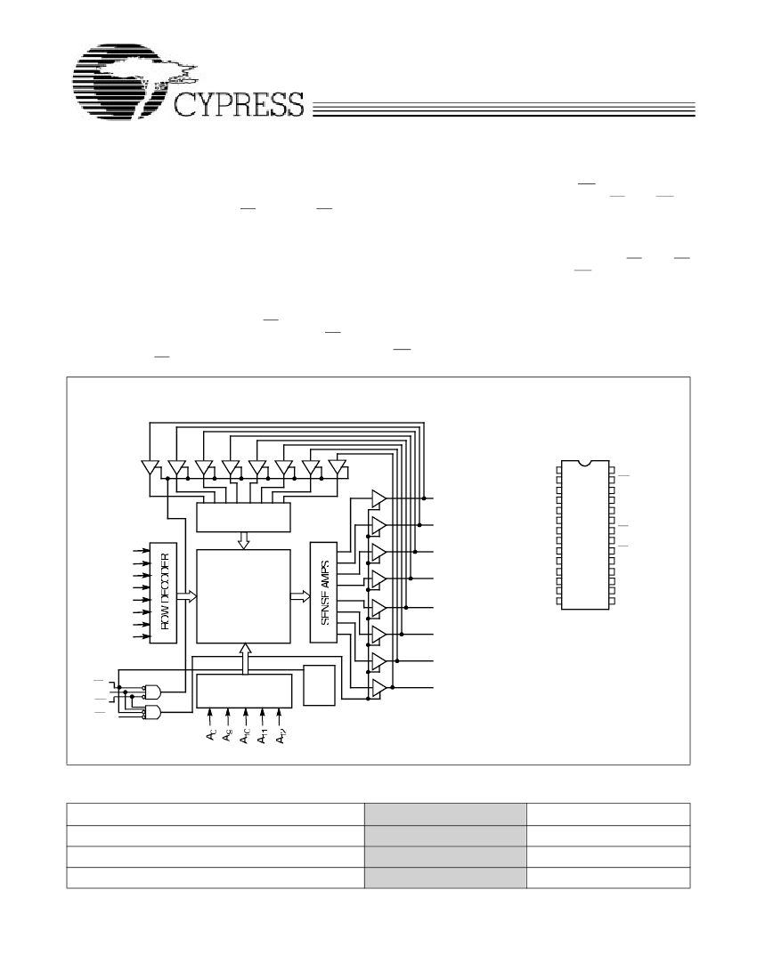
Logic Block Diagram
Pin Configuration
SOIC
Top View
NC
A
4
A
5
A
6
A
7
A
8
A
9
A
10
A
11
A
12
I/O
0
I/O
1
I/O
2
GND
1
2
3
4
5
6
7
8
9
10
11
12
13
14
28
27
26
25
24
23
22
21
20
19
18
17
16
15
V
CC
WE
CE
2
A
3
A
2
A
1
OE
A
0
CE
1
I/O
7
I/O
6
I/O
5
I/O
4
I/O
3
CY6264-2
I/O
0
INPUT BUFFER
I/O
1
A
1
A
2
A
3
A
4
A
5
A
6
A
7
A
8
I/O
2
I/O
3
256 x 32 x 8
ARRA
Y
I/O
4
I/O
5
I/O
6
CE
1
CE
2
WE
OE
CY6264-1
COLUMN DECODER
POWER
DOWN
I/O
7
Selection Guide
CY6264-55
Maximum Access Time (ns)
Maximum Operating Current (mA)
Maximum Standby Current (mA)
Shaded area contains advanced information.
CY6264-70
70
100
20/15
55
100
20/15
Cypress Semiconductor Corporation
鈥?/div>
3901 North First Street
鈥?/div>
San Jose
鈥?/div>
CA 95134 鈥?/div>
408-943-2600
October 1994 鈥?Revised June 1996


 1
1
 2
2
 3
3
 4
4
 5
5
 6
6
 7
7
 8
8
