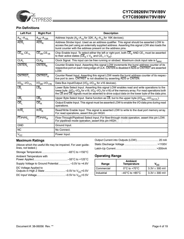
鈥?/div>
鈥?Supported in Flow-Through and Pipelined modes
Dual Chip Enables for easy depth expansion
Upper and Lower Byte Controls for Bus Matching
Automatic power-down
Commercial and Industrial temperature ranges
Available in 100-pin TQFP
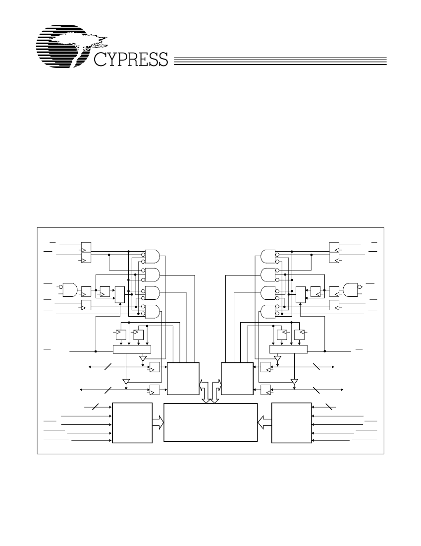
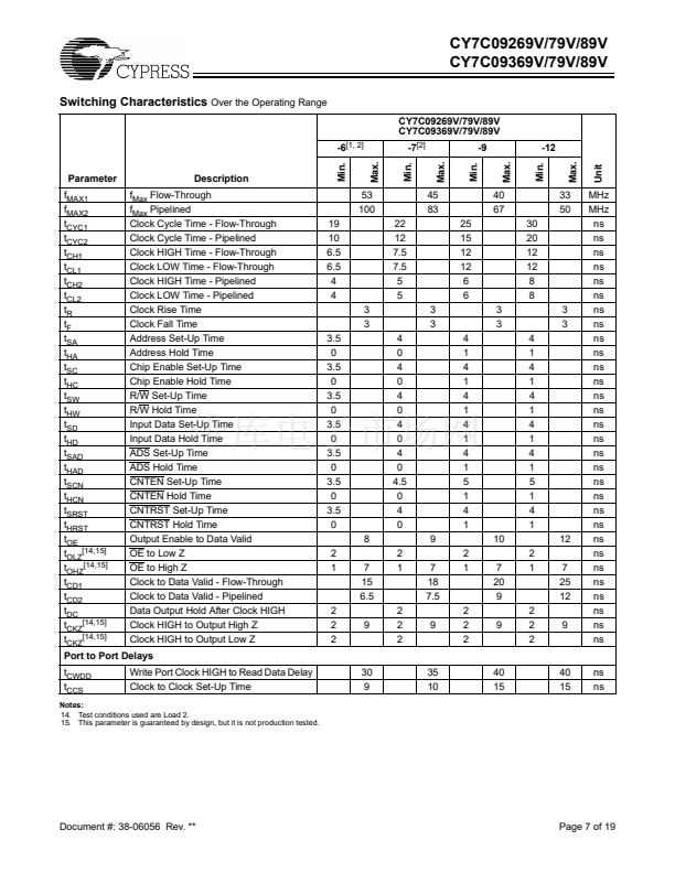
Logic Block Diagram
R/W
L
UB
L
R/W
R
UB
R
CE
0L
CE
1L
LB
L
OE
L
1
0/1
1
0/1
0
0
CE
0R
CE
1R
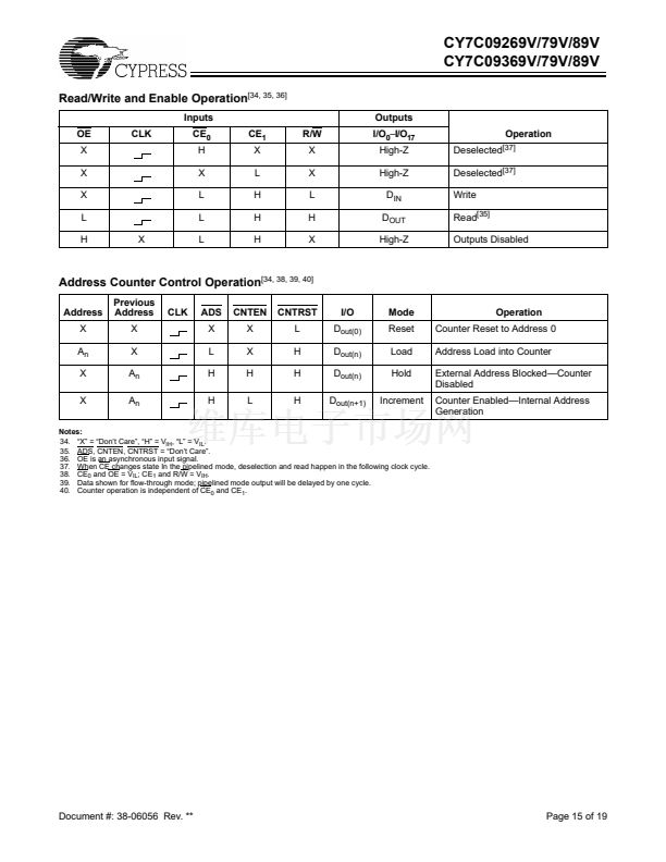
LB
R
OE
R
FT/Pipe
L
[3]
0/1
1b 0b 1a 0a
b
a
0a 1a 0b 1b
a
b
0/1
FT/Pipe
R
8/9
[3]
8/9
I/O
8/9L
鈥揑/O
15/17L
[4]
I/O
8/9R
鈥揑/O
15/17R
8/9
I/O
Control
I/O
Control
8/9
14/15/16
I/O
0L
鈥揑/O
7/8L
A
0L
鈥揂
13/14/15L
CLK
L
ADS
L
CNTEN
L
CNTRST
L
[5]
I/O
0R
鈥揑/O
7/8R
14/15/16
[4]
Counter/
Address
Register
Decode
True Dual-Ported
RAM Array
Counter/
Address
Register
Decode
A
0R
鈥揂
13/14/15R
CLK
R
ADS
R
CNTEN
R
CNTRST
R
[5]
Notes:
1. Call for availability.
2. See page 6 for Load Conditions.
3. I/O
8
鈥揑/O
15
for x16 devices; I/O
9
鈥揑/O
17
for x18 devices.
4. I/O
0
鈥揑/O
7
for x16 devices. I/O
0
鈥揑/O
8
for x18 devices.
5. A
0
鈥揂
13
for 16K; A
0
鈥揂
14
for 32K; A
0
鈥揂
15
for 64K devices.
For the most recent information, visit the Cypress web site at www.cypress.com
Cypress Semiconductor Corporation
鈥?3901 North First Street 鈥?San Jose 鈥?CA 95134 鈥?408-943-2600
Document #: 38-06056 Rev. **
Revised September 21, 2001


 1
1
 2
2
 3
3
 4
4
 5
5
 6
6
 7
7
 8
8
 9
9
 10
10
 11
11
 12
12
 13
13
 14
14
 15
15
 16
16
 17
17
 18
18
 19
19
