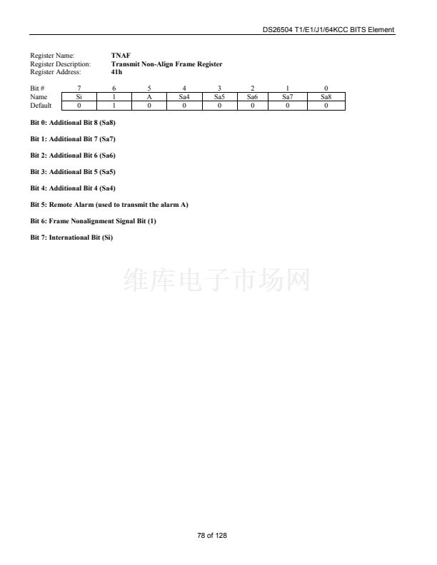
DS26504
T1/E1/J1/64KCC BITS Element
www.maxim-ic.com
GENERAL DESCRIPTION
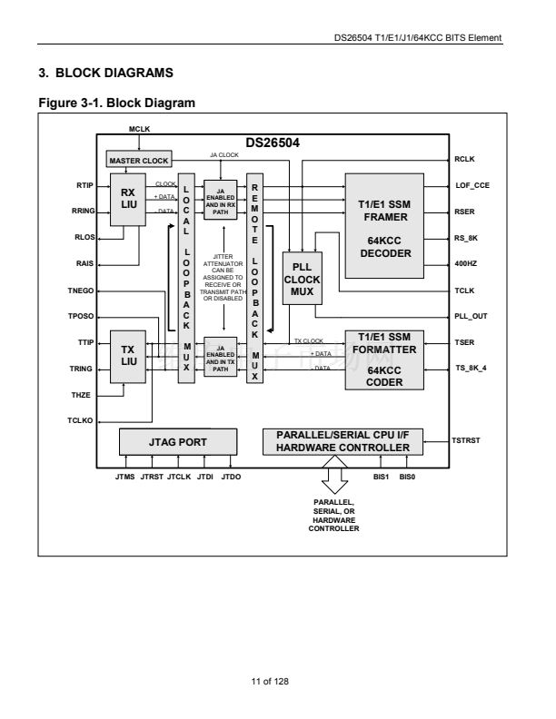
The DS26504 is a building-integrated timing-supply
(BITS) clock-recovery element. It also functions as a
basic T1/E1 transceiver. The receiver portion can
recover a clock from T1, E1, 64kHz composite clock
(64KCC), and 6312kHz synchronization timing
interfaces. In T1 and E1 modes, the Synchronization
Status Message (SSM) can also be recovered. The
transmit portion can directly interface to T1, E1, or
64KCC synchronization interfaces as well as source
the SSM in T1 and E1 modes. The DS26504 can
translate between any of the supported inbound
synchronization clock rates to any supported
outbound rate. The DS26504 can also accept an 8kHz
as well as a 19.44MHz reference clock. A separate
output is provided to source a 6312kHz clock. The
device is controlled through a parallel, serial, or
hardware controller port.
搂
搂
搂
搂
搂
搂
搂
搂
搂
搂
搂
搂
搂
搂
搂
APPLICATIONS
BITS Timing
Rate Conversion
FEATURES
搂
搂
搂
搂
搂
搂
搂
搂
搂
搂
Accepts 8kHz and 19.44MHz References in
Addition to T1, E1, and 64kHz Composite Clock
GR378 Composite Clock Compliant
G.703 2048kHz Synchronization Interface
Compliant
G.703 64kHz Option A & B Centralized Clock
Synchronization Interface Compliant
G.703 64kHz Japanese Composite Clock
Synchronization Interface Compliant
G.703 6312kHz Japanese Synchronization
Interface Compliant
Interfaces to Standard T1/J1 (1.544MHz) and E1
(2.048MHz)
Interface to CMI-Coded T1/J1 and E1
T1/E1 Transmit Payload Clock Output
Short- and Long-Haul Line Interface
Transmit and Receive T1 BOC SSM Messages
with Receive Message Change of State and
Validation Indication
Transmit and Receive E1 Sa(n) Bit SSM
Messages with Receive Message Change of State
Indication
Crystal-Less Jitter Attenuator with Bypass Mode
for T1 and E1 Operation
Fully Independent Transmit and Receive
Functionality
Internal Software-Selectable Receive and
Transmit Side Termination for
75鈩?100鈩?110鈩?120鈩?133鈩?/div>
Monitor Mode for Bridging Applications
Accepts 16.384MHz, 12.8MHz, 8.192MHz,
4.096MHz, 2.048MHz, or 1.544MHz Master
Clock
64kHz, 8kHz, and 400Hz Outputs in Composite
Clock Mode
8-Bit Parallel Control Port, Multiplexed or
Nonmultiplexed, Intel or Motorola
Serial (SPI) Control Port and Hardware Control
Mode
Provides LOS, AIS, and LOF Indications through
Hardware Output Pins
Fast Transmitter Output Disable through Device
Pin for Protection Switching
IEEE 1149.1 JTAG Boundary Scan
3.3V Supply with 5V Tolerant Inputs and
Outputs
Pin and Software Compatible with the DS26502
and DS26503
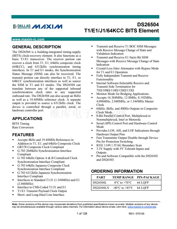
ORDERING INFORMATION
PART
DS26504L
DS26504LN
TEMP RANGE PIN-PACKAGE
0掳C to +70掳C
-40掳C to +85掳C
64 LQFP
64 LQFP
Note:
Some revisions of this device may incorporate deviations from published specifications known as errata. Multiple revisions of any device
may be simultaneously available through various sales channels. For information about device errata, click here:
www.maxim-ic.com/errata.
1 of 128
REV: 070105


 1
1
 2
2
 3
3
 4
4
 5
5
 6
6
 7
7
 8
8
 9
9
 10
10
 11
11
 12
12
 13
13
 14
14
 15
15
 16
16
 17
17
 18
18
 19
19
 20
20
 21
21
 22
22
 23
23
 24
24
 25
25
 26
26
 27
27
 28
28
 29
29
 30
30
 31
31
 32
32
 33
33
 34
34
 35
35
 36
36
 37
37
 38
38
 39
39
 40
40
 41
41
 42
42
 43
43
 44
44
 45
45
 46
46
 47
47
 48
48
 49
49
 50
50
 51
51
 52
52
 53
53
 54
54
 55
55
 56
56
 57
57
 58
58
 59
59
 60
60
 61
61
 62
62
 63
63
 64
64
 65
65
 66
66
 67
67
 68
68
 69
69
 70
70
 71
71
 72
72
 73
73
 74
74
 75
75
 76
76
 77
77
 78
78
 79
79
 80
80
 81
81
 82
82
 83
83
 84
84
 85
85
 86
86
 87
87
 88
88
 89
89
 90
90
 91
91
 92
92
 93
93
 94
94
 95
95
 96
96
 97
97
 98
98
 99
99
 100
100
 101
101
 102
102
 103
103
 104
104
 105
105
 106
106
 107
107
 108
108
 109
109
 110
110
 111
111
 112
112
 113
113
 114
114
 115
115
 116
116
 117
117
 118
118
 119
119
 120
120
 121
121
 122
122
 123
123
 124
124
 125
125
 126
126
 127
127
 128
128
