2SK1381
TOSHIBA Field Effect Transistor Silicon N Channel MOS Type (L
2
鈭捪€鈭扢OSIII)
2SK1381
Relay Drive, Motor Drive and DC鈭扗C Converter
Applications
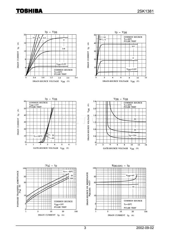
4 V gate drive
Low drain鈭抯ource ON resistance
High forward transfer admittance
Low leakage current
Enhancement鈭抦ode
: R
DS (ON)
= 25 m鈩?(typ.)
: |Y
fs
| = 33 S (typ.)
: I
DSS
=
100
碌A (max) (V
DS
=
100
V)
: V
th
= 0.8~2.0 V (V
DS
=
10
V, I
D
=
1
mA)
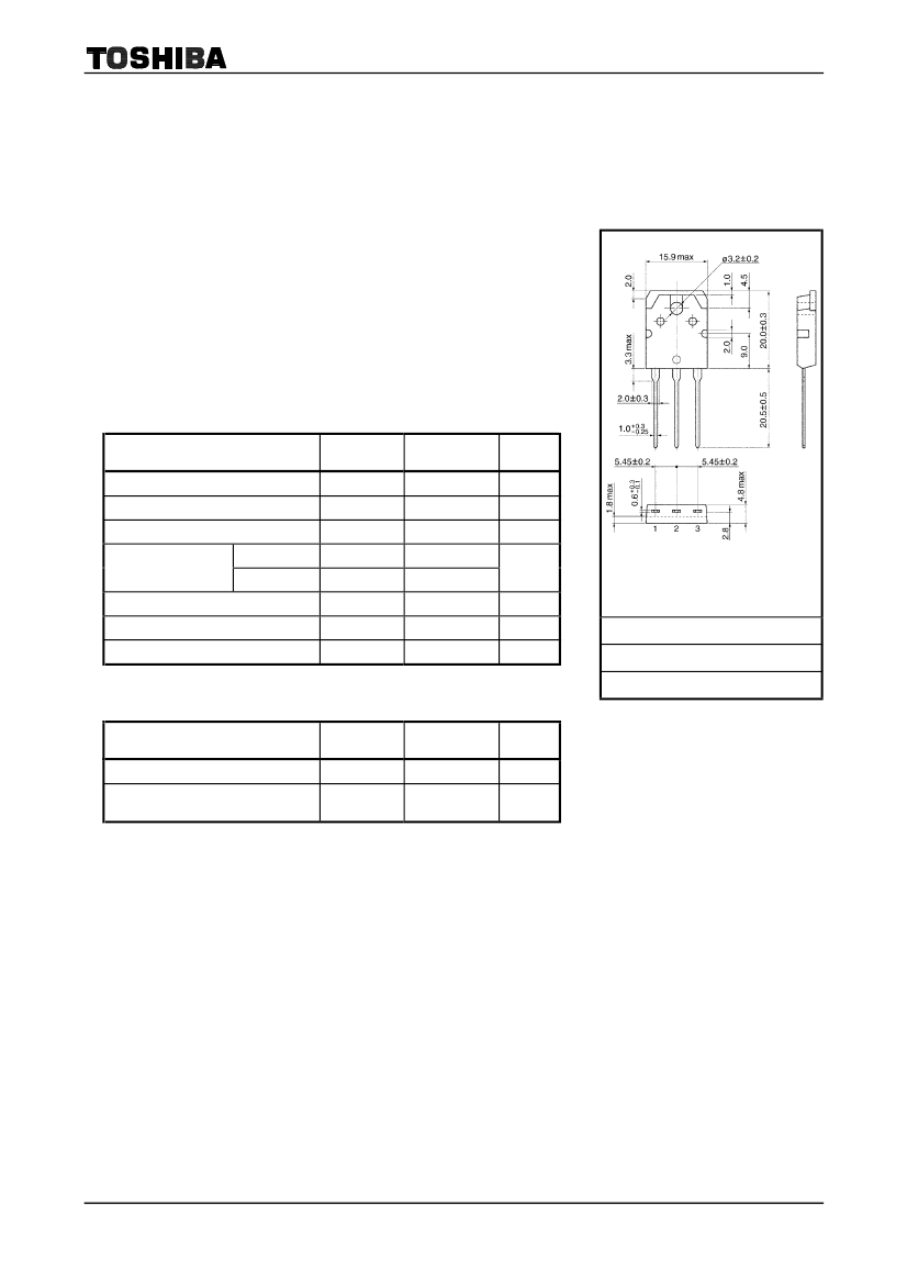
Unit: mm
Maximum Ratings
(Ta = 25掳C)
Characteristics
Drain鈭抯ource voltage
Drain鈭抔ate voltage (R
GS
= 20 k鈩?
Gate鈭抯ource voltage
Drain current
DC
(Note 1)
Symbol
V
DSS
V
DGR
V
GSS
I
D
I
DP
P
D
T
ch
T
stg
Rating
100
100
卤20
50
200
150
150
鈭?5~150
Unit
V
V
V
A
W
掳C
掳C
1. GATE
2. DRAIN (HEAT SINK)
3. SOURCE
Pulse (Note 1)
Drain power dissipation (Tc = 25掳C)
Channel temperature
Storage temperature range
JEDEC
JEITA
TOSHIBA
鈥?/div>
鈥?/div>
2-16C1B
Thermal Characteristics
Characteristics
Thermal resistance, channel to case
Thermal resistance, channel to
ambient
Symbol
R
th (ch鈭抍)
R
th (ch鈭抋)
Max
0.833
50
Unit
掳C / W
掳C / W
Weight: 4.6 g (typ.)
Note 1: Please use devices on condition that the channel temperature is below 150掳C.
This transistor is an electrostatic sensitive device.
Please handle with caution.
1
2002-09-02


 1
1
 2
2
 3
3
 4
4
 5
5
 6
6
