19-2544; Rev 1; 12/02
LVECL/LVPECL 1:15 Differential
Divide-by-1/Divide-by-2 Clock Driver
General Description
The MAX9322 low-skew 1:15 differential clock driver
reproduces or divides one of two differential input clocks
at 15 differential outputs. An input multiplexer selects from
one of two input clocks with input switching frequency in
excess of 1.0GHz. The 15 outputs are arranged in four
banks with 2, 3, 4, and 6 outputs, respectively. Each
output bank is individually programmable to provide a
divide-by-1 or divide-by-2 frequency function.
The MAX9322 operates in LVPECL systems with a
+2.375V to +3.8V supply or in LVECL systems with a
-2.375V to -3.8V supply. A V
BB
reference output pro-
vides compatibility with single-ended clock input sig-
nals and a master reset input provides a simultaneous
reset on all outputs.
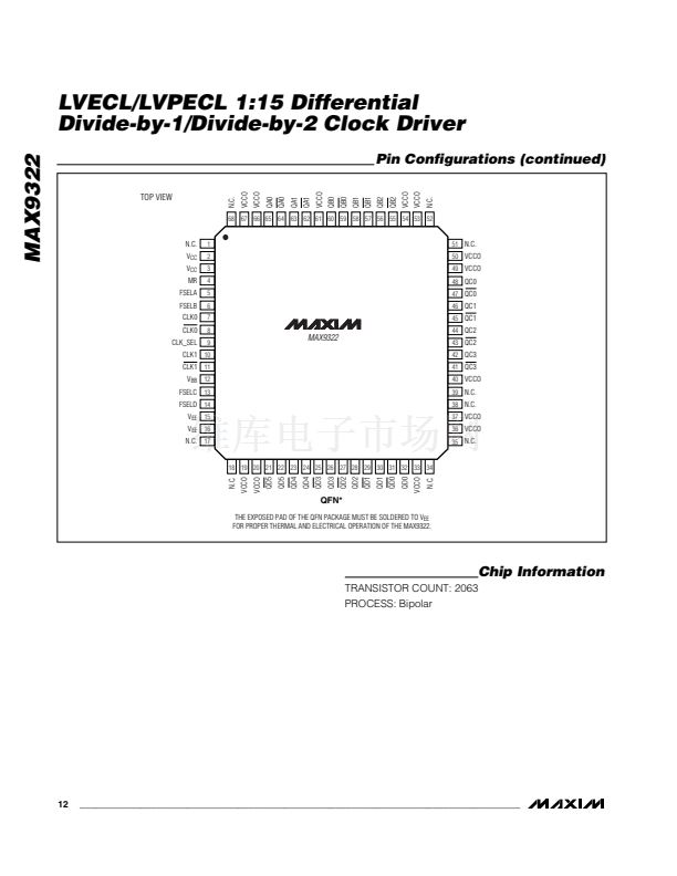
The MAX9322 is available in 52-pin TQFP and 68-pin
QFN packages and is specified for operation over
-40掳C to +85掳C. For 1:10 clock drivers, refer to the
MAX9311/MAX9313 data sheet. For 1:5 clock drivers,
refer to the MAX9316 data sheet.
o
300mV Differential Output at 1.0GHz
o
900ps Propagation Delay
o
Selectable Divide-by-1 or Divide-by-2 Frequency
Outputs
o
Multiplexed 2:1 Input Function
o
LVECL Operation from V
EE
= -2.375V to -3.8V
o
LVPECL Operation from V
CC
= +2.375V to +3.8V
o
ESD Protection: > 2kV Human Body Model
Features
o
1.2ps (RMS) Maximum Random Jitter
MAX9322
Ordering Information
PART
MAX9322ECY
MAX9322ETK*
TEMP RANGE
-40掳C to +85掳C
-40掳C to +85掳C
PIN-
PACKAGE
52 TQFP
68 QFN
Applications
Precision Clock Distribution
Low-Jitter Data Repeaters
Central-Office Backplane Clock Distribution
DSLAM Backplane
Base Stations
ATE
*Future
product鈥攃ontact factory for availability.
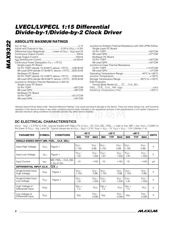
Pin Configurations
TOP VIEW
VCCO
VCCO
VCCO
40
39
VCCO
2
38
QC0
3
37
QC0
4
36
QC1
5
35
QC1
6
7
8
32
QC3
9
31
QC3
30
VCCO
29
N.C.
34
QC2
33
QC2
28
N.C.
27
VCCO
26
QA0
QA0
QA1
QA1
QB0
QB0
QB1
QB1
QB2
42
24
52
51
50
49
48
47
46
45
44
43
41
V
CC
MR
FSELA
1
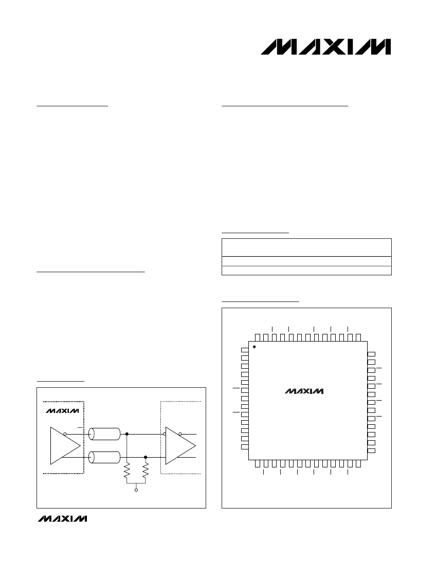
Typical Operating Circuit
FSELB
CLK0
CLK0
CLK_SEL
CLK1
MAX9322
MAX9322
Z
O
= 50鈩?/div>
Q_
RECEIVER
CLK1
V
BB
10
FSELC
11
FSELD
12
Z
O
= 50鈩?/div>
Q_
V
EE
13
14
15
16
17
18
19
20
21
22
23
QD5
QD5
QD4
QD4
QD3
QD3
QD2
QD2
QD1
QD1
QD0
QB2
25
50鈩?/div>
50鈩?/div>
VCCO
TQFP
V
TT
= V
CC
- 2.0V
Pin Configurations continued at end of data sheet.
________________________________________________________________
Maxim Integrated Products
QD0
1
For pricing, delivery, and ordering information, please contact Maxim/Dallas Direct! at
1-888-629-4642, or visit Maxim鈥檚 website at www.maxim-ic.com.


 1
1
 2
2
 3
3
 4
4
 5
5
 6
6
 7
7
 8
8
 9
9
 10
10
 11
11
 12
12
 13
13
