Power Dissipation, per Package鈥?/div>
Storage Temperature
mA
mW
Tstg
TL
鈥?65 to + 150
260
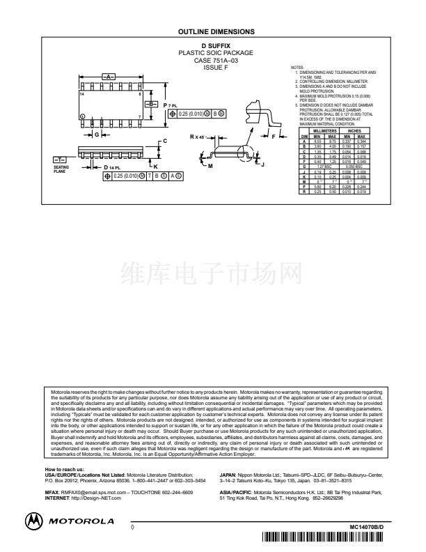
D SUFFIX
SOIC
CASE 751A
ORDERING INFORMATION
MC14XXXBCP
MC14XXXBCL
MC14XXXBD
Plastic
Ceramic
SOIC
TA = 鈥?55掳 to 125掳C for all packages.
_
C
_
C
Lead Temperature (8鈥揝econd Soldering)
* Maximum Ratings are those values beyond which damage to the device may occur.
鈥燭emperature Derating:
Plastic 鈥淧 and D/DW鈥?Packages: 鈥?7.0 mW/
_
C From 65
_
C To 125
_
C
Ceramic 鈥淟鈥?Packages: 鈥?12 mW/
_
C From 100
_
C To 125
_
C
20 ns
VDD
IDD
Vin
*
CL
* Inverted output on MC14077B only.
Vin
90%
50%
10%
1/f
50% DUTY CYCLE
20 ns
VDD
VSS
MC14070B
QUAD Exclusive OR
Gate
1
3
2
5
4
6
8
10
9
12
11
13
MC14077B
QUAD Exclusive NOR
Gate
1
3
2
5
4
6
8
10
9
12
11
13
VDD = PIN 14
VSS = PIN 7
(BOTH DEVICES)
20 ns
Figure 1. Power Dissipation Test Circuit and Waveform
VDD
PULSE
GENERATOR
*
#
VSS
CL
20 ns
INPUT
tPHL
OUTPUT
90%
50%
10%
90%
50%
10%
tPLH
PIN ASSIGNMENT
VDD
VSS
VOH
IN 1A
IN 2A
OUTA
OUTB
IN 1B
IN 2B
VSS
1
2
3
4
5
6
7
14
13
12
11
10
9
8
VDD
IN 2D
IN 1D
OUTD
OUTC
IN 2C
IN 1C
tTHL
* Inverted output on MC14077B only.
#Connect unused input to VDD for MC14070B, to VSS for MC14077B.
VOL
tTLH
Figure 2. Switching Time Test Circuit and Waveforms
REV 3
1/94
漏
MOTOROLA CMOS LOGIC DATA
Motorola, Inc. 1995
MC14070B MC14077B
1


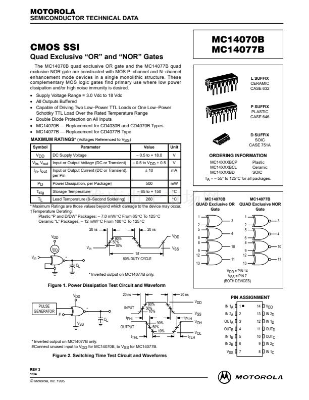 1
1
 2
2
 3
3
 4
4
