鈥?/div>
Six Low Skew Outputs
Synchronous Output Enables for Power Management
Low Voltage Operation
XTAL Oscillator Interface
16-Lead SOIC Package
5.0V Tolerant Enable Inputs
16
1
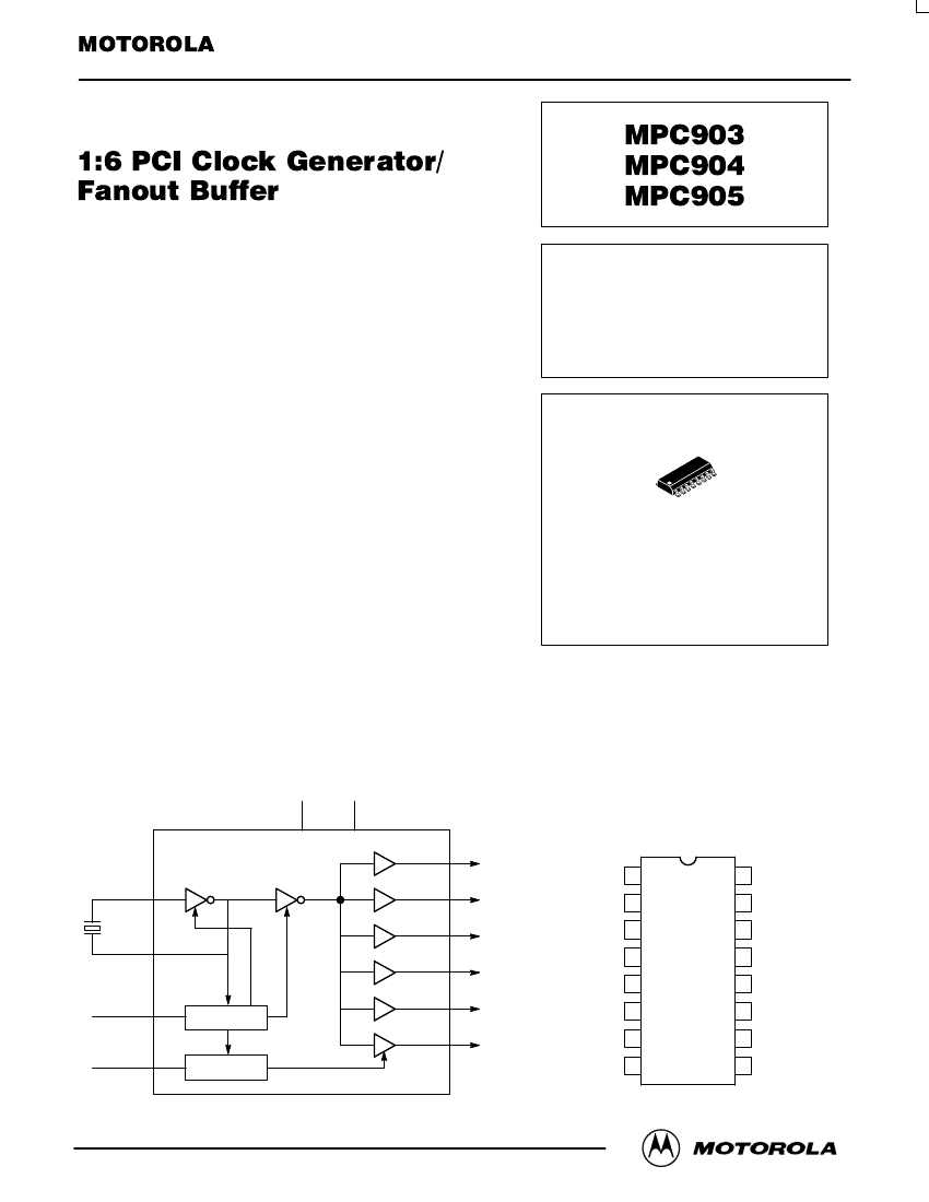
The MPC903/904/905 device is targeted for PCI bus or processor bus
environments with up to 12 clock loads. Each of the six outputs on the
MPC903/904/905 can drive two series terminated 50鈩?transmission
lines. This capability effectively makes the MPC903/904/905 a 1:12
fanout buffer.
D SUFFIX
PLASTIC SOIC PACKAGE
CASE 751B-05
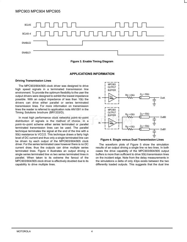
The MPC903 offers two synchronous enable inputs to allow users
flexibility in developing power management features for their designs.
Both enable signals are active HIGH inputs. A logic 鈥?鈥?on the Enable1
input will pull all of the outputs into the logic 鈥?鈥?state and shut down the
internal oscillator for a zero power sleep state. A logic 鈥?鈥?on the Enable2
input will disable only the BCLK5 output. The Enable2 input can be used to disable any high power device for system power
savings during periods of inactivity. Both enable inputs are synchronized internal to the chip so that the output disabling will
happen only when the outputs are already LOW. This feature guarantees no runt pulses will be generated during enabling and
disabling. Note that when the MPC903 is re-enabled via the Enable1 pin, the user must allow for the oscillator to regain stability.
Thus, the re-enabling of the chip cannot occur instantaneously. The MPC904 and MPC905 Enable functions are slightly different
than the 903 and are outlined in the function tables on the following page.
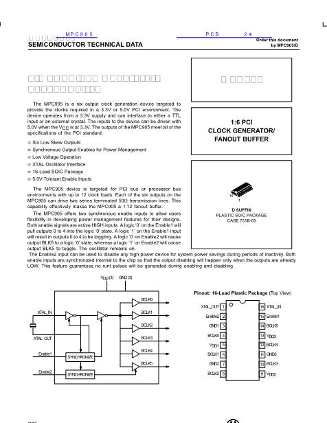
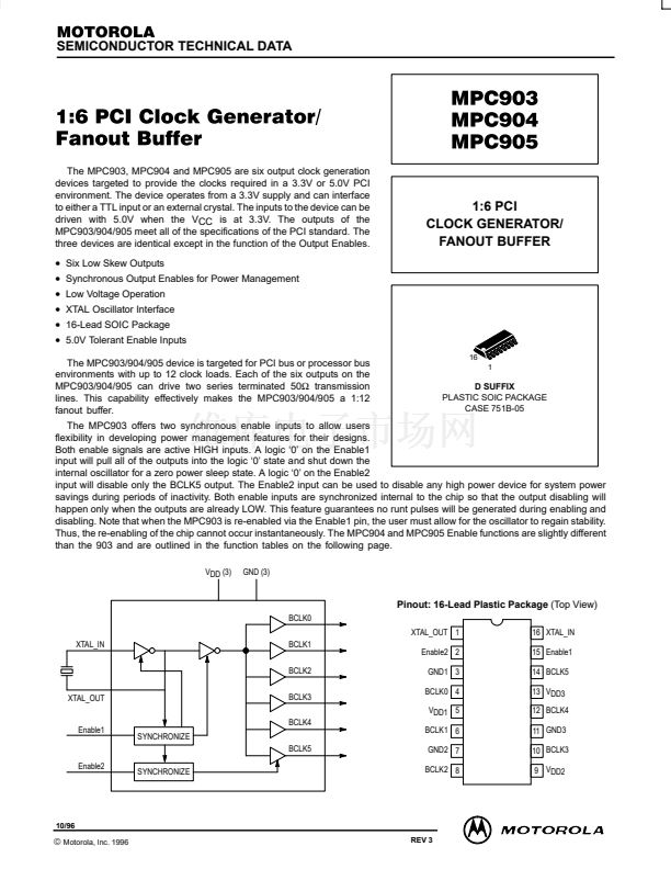
VDD (3)
GND (3)
Pinout: 16-Lead Plastic Package
(Top View)
BCLK0
XTAL_OUT 1
XTAL_IN
BCLK1
BCLK2
XTAL_OUT
BCLK3
BCLK4
SYNCHRONIZE
BCLK5
Enable2
SYNCHRONIZE
Enable2 2
GND1 3
BCLK0 4
VDD1 5
Enable1
BCLK1 6
GND2 7
BCLK2 8
16 XTAL_IN
15 Enable1
14 BCLK5
13 VDD3
12 BCLK4
11 GND3
10 BCLK3
9 VDD2
10/96
漏
Motorola, Inc. 1996
1
REV 3


 1
1
 2
2
 3
3
 4
4
 5
5
 6
6
