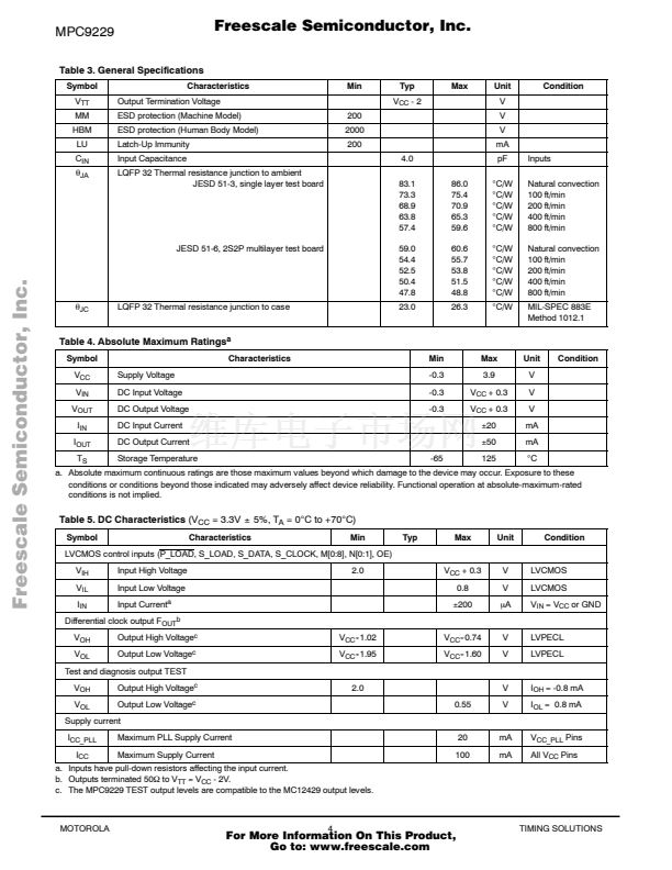
鈥?/div>
Features
25 MHz to 400 MHz synthesized clock output signal
Differential PECL output
LVCMOS compatible control inputs
On-chip crystal oscillator for reference frequency generation
3.3V power supply
Fully integrated PLL
Minimal frequency overshoot
Serial 3-wire programming interface
Parallel programming interface for power-up
32 lead LQFP and 28 PLCC packaging
SiGe Technology
Ambient temperature range 0掳C to +70掳C
Pin and function compatible to the MC12429
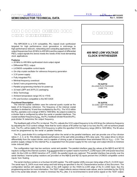
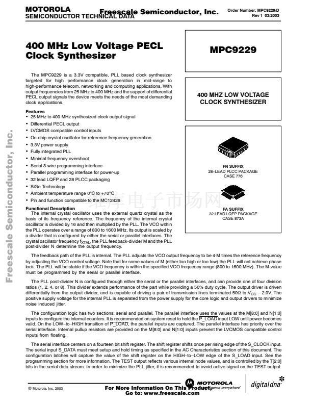
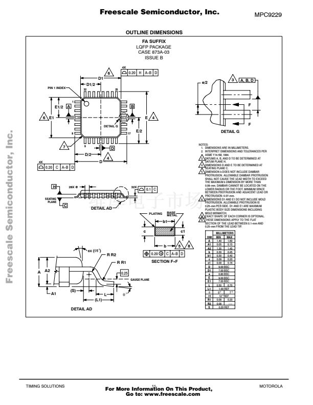
FA SUFFIX
32 LEAD LQFP PACKAGE
CASE 873A
FN SUFFIX
28-
-LEAD PLCC PACKAGE
CASE 776
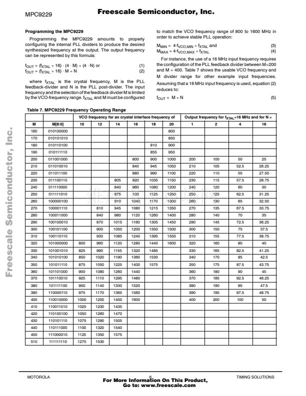
Functional Description
The internal crystal oscillator uses the external quartz crystal as the
basis of its frequency reference. The frequency of the internal crystal
oscillator is divided by 16 and then multiplied by the PLL. The VCO within
the PLL operates over a range of 800 to 1600 MHz. Its output is scaled by
a divider that is configured by either the serial or parallel interfaces. The
crystal oscillator frequency f
XTAL
, the PLL feedback-divider M and the PLL
post-divider N determine the output frequency.
The feedback path of the PLL is internal. The PLL adjusts the VCO output frequency to be 4鈰匨 times the reference frequency
by adjusting the VCO control voltage. Note that for some values of M (either too high or too low) the PLL will not achieve phase
lock. The PLL will be stable if the VCO frequency is within the specified VCO frequency range (800 to 1600 MHz). The M-value
must be programmed by the serial or parallel interface.
The PLL post-divider N is configured through either the serial or the parallel interfaces, and can provide one of four division
ratios (1, 2, 4, or 8). This divider extends performance of the part while providing a 50% duty cycle. The output driver is driven
differentially from the output divider, and is capable of driving a pair of transmission lines terminated 50鈩?to V
CC
鈥?2.0V. The
positive supply voltage for the internal PLL is separated from the power supply for the core logic and output drivers to minimize
noise induced jitter.
The configuration logic has two sections: serial and parallel. The parallel interface uses the values at the M[8:0] and N[1:0]
inputs to configure the internal counters. It is recommended on system reset to hold the P_LOAD input LOW until power becomes
valid. On the LOW鈥搕o鈥揌IGH transition of P_LOAD, the parallel inputs are captured. The parallel interface has priority over the
serial interface. Internal pullup resistors are provided on the M[8:0] and N[1:0] inputs prevent the LVCMOS compatible control
inputs from floating.
The serial interface centers on a fourteen bit shift register. The shift register shifts once per rising edge of the S_CLOCK input.
The serial input S_DATA must meet setup and hold timing as specified in the AC Characteristics section of this document. The
configuration latches will capture the value of the shift register on the HIGH鈥搕o鈥揕OW edge of the S_LOAD input. See the
programming section for more information. The TEST output reflects various internal node values, and is controlled by the T[2:0]
bits in the serial data stream. In order to minimize the PLL jitter, it is recommended to avoid active signal on the TEST output.
铮?/div>
Motorola, Inc. 2003
For More Information On This Product,
Go to: www.freescale.com


 1
1
 2
2
 3
3
 4
4
 5
5
 6
6
 7
7
 8
8
 9
9
 10
10
 11
11
 12
12
