鈥?/div>
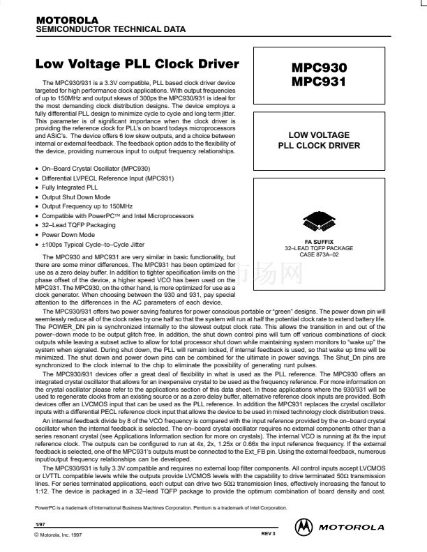
On鈥揃oard Crystal Oscillator (MPC930)
Differential LVPECL Reference Input (MPC931)
Fully Integrated PLL
Output Shut Down Mode
Output Frequency up to 150MHz
Compatible with PowerPC鈩?and Intel Microprocessors
32鈥揕ead TQFP Packaging
Power Down Mode
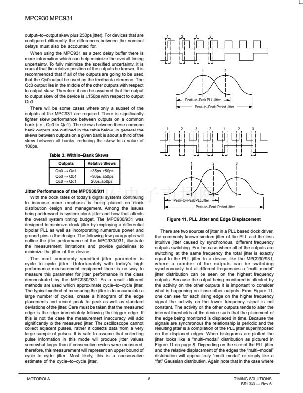
卤100ps
Typical Cycle鈥搕o鈥揅ycle Jitter
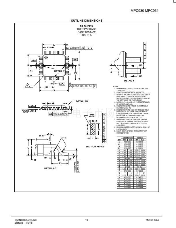
FA SUFFIX
32鈥揕EAD TQFP PACKAGE
CASE 873A鈥?2
The MPC930 and MPC931 are very similar in basic functionality, but
there are some minor differences. The MPC931 has been optimized for
use as a zero delay buffer. In addition to tighter specification limits on the
phase offset of the device, a higher speed VCO has been used on the
MPC931. The MPC930, on the other hand, is more optimized for use as a
clock generator. When choosing between the 930 and 931, pay special
attention to the differences in the AC parameters of each device.
The MPC930/931 offers two power saving features for power conscious portable or 鈥済reen鈥?designs. The power down pin will
seemlessly reduce all of the clock rates by one half so that the system will run at half the potential clock rate to extend battery life.
The POWER_DN pin is synchronized internally to the slowest output clock rate. This allows the transition in and out of the
power鈥揹own mode to be output glitch free. In addition, the shut down control pins will turn off various combinations of clock
outputs while leaving a subset active to allow for total processor shut down while maintaining system monitors to 鈥渨ake up鈥?the
system when signaled. During shut down, the PLL will remain locked, if internal feedback is used, so that wake up time will be
minimized. The shut down and power down pins can be combined for the ultimate in power savings. The Shut_Dn pins are
synchronized to the clock internal to the chip to eliminate the possibility of generating runt pulses.
The MPC930/931 devices offer a great deal of flexibility in what is used as the PLL reference. The MPC930 offers an
integrated crystal oscillator that allows for an inexpensive crystal to be used as the frequency reference. For more information on
the crystal oscillator please refer to the applications section of this data sheet. In those applications where the 930/931 will be
used to regenerate clocks from an existing source or as a zero delay buffer, alternative reference clock inputs are provided. Both
devices offer an LVCMOS input that can be used as the PLL reference. In addition the MPC931 replaces the crystal oscillator
inputs with a differential PECL reference clock input that allows the device to be used in mixed technology clock distribution trees.
An internal feedback divide by 8 of the VCO frequency is compared with the input reference provided by the on鈥揵oard crystal
oscillator when the internal feedback is selected. The on鈥揵oard crystal oscillator requires no external components other than a
series resonant crystal (see Applications Information section for more on crystals). The internal VCO is running at 8x the input
reference clock. The outputs can be configured to run at 4x, 2x, 1.25x or 0.66x the input reference frequency. If the external
feedback is selected, one of the MPC931鈥檚 outputs must be connected to the Ext_FB pin. Using the external feedback, numerous
input/output frequency relationships can be developed.
The MPC930/931 is fully 3.3V compatible and requires no external loop filter components. All control inputs accept LVCMOS
or LVTTL compatible levels while the outputs provide LVCMOS levels with the capability to drive terminated 50鈩?transmission
lines. For series terminated applications, each output can drive two 50鈩?transmission lines, effectively increasing the fanout to
1:12. The device is packaged in a 32鈥搇ead TQFP package to provide the optimum combination of board density and cost.
PowerPC is a trademark of International Business Machines Corporation. Pentium is a trademark of Intel Corporation.
1/97
漏
Motorola, Inc. 1997
1
REV 3


 1
1
 2
2
 3
3
 4
4
 5
5
 6
6
 7
7
 8
8
 9
9
 10
10
 11
11
 12
12
 13
13
 14
14
