鈥?/div>
1:6 PLL based low-voltage clock generator
3.3 V power supply
Generates clock signals up to 240 MHz
Maximum output skew of 150 ps
Differential LVPECL reference clock input
Alternative LVCMOS PLL reference clock input
Internal and external PLL feedback
Supports zero-delay operation in external feedback mode
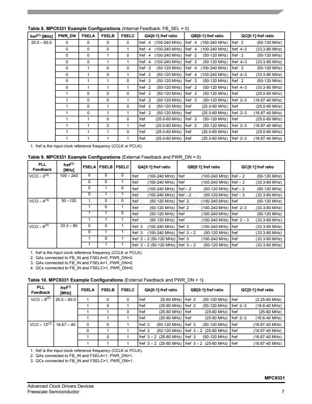
PLL multiplies the reference clock by 4x, 3x, 2x, 1x, 4/3x, 3/2x, 2/3x, x/2, x/3
or x/4
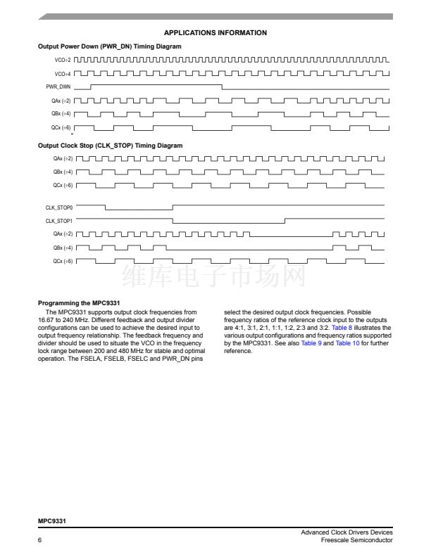
Synchronous output clock stop in logic low eliminates output runt pulses
Power_down feature reduces output clock frequency
Drives up to 12 clock lines
32-lead LQFP packaging
32-lead Pb-free Package Available
Ambient temperature range 0掳C to +70掳C
Internal Power-Up Reset
Pin and function compatible to the MPC931
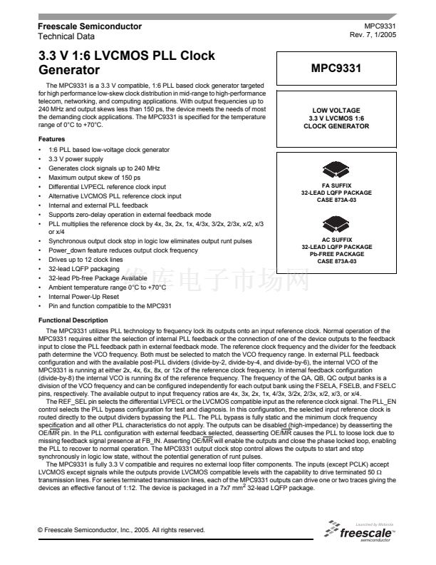
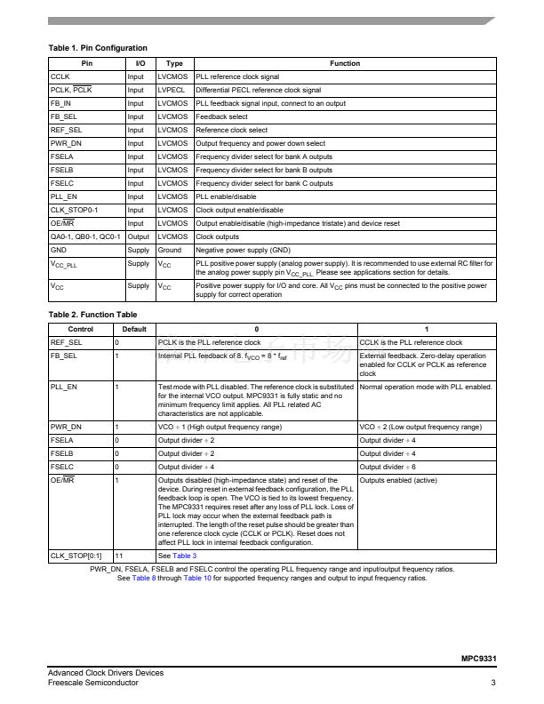
MPC9331
LOW VOLTAGE
3.3 V LVCMOS 1:6
CLOCK GENERATOR
FA SUFFIX
32-LEAD LQFP PACKAGE
CASE 873A-03
AC SUFFIX
32-LEAD LQFP PACKAGE
Pb-FREE PACKAGE
CASE 873A-03
Functional Description
The MPC9331 utilizes PLL technology to frequency lock its outputs onto an input reference clock. Normal operation of the
MPC9331 requires either the selection of internal PLL feedback or the connection of one of the device outputs to the feedback
input to close the PLL feedback path in external feedback mode. The reference clock frequency and the divider for the feedback
path determine the VCO frequency. Both must be selected to match the VCO frequency range. In external PLL feedback
configuration and with the available post-PLL dividers (divide-by-2, divide-by-4, and divide-by-6), the internal VCO of the
MPC9331 is running at either 2x, 4x, 6x, 8x, or 12x of the reference clock frequency. In internal feedback configuration
(divide-by-8) the internal VCO is running 8x of the reference frequency. The frequency of the QA, QB, QC output banks is a
division of the VCO frequency and can be configured independently for each output bank using the FSELA, FSELB, and FSELC
pins, respectively. The available output to input frequency ratios are 4x, 3x, 2x, 1x, 4/3x, 3/2x, 2/3x, x/2, x/3, or x/4.
The REF_SEL pin selects the differential LVPECL or the LVCMOS compatible input as the reference clock signal. The PLL_EN
control selects the PLL bypass configuration for test and diagnosis. In this configuration, the selected input reference clock is
routed directly to the output dividers bypassing the PLL. The PLL bypass is fully static and the minimum clock frequency
specification and all other PLL characteristics do not apply. The outputs can be disabled (high-impedance) by deasserting the
OE/MR pin. In the PLL configuration with external feedback selected, deasserting OE/MR causes the PLL to loose lock due to
missing feedback signal presence at FB_IN. Asserting OE/MR will enable the outputs and close the phase locked loop, enabling
the PLL to recover to normal operation. The MPC9331 output clock stop control allows the outputs to start and stop
synchronously in logic low state, without the potential generation of runt pulses.
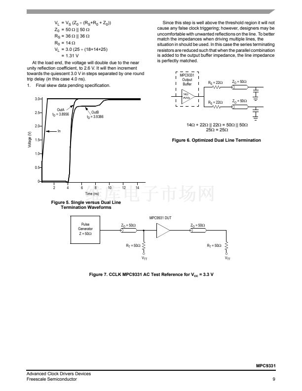
The MPC9331 is fully 3.3 V compatible and requires no external loop filter components. The inputs (except PCLK) accept
LVCMOS except signals while the outputs provide LVCMOS compatible levels with the capability to drive terminated 50
鈩?/div>
transmission lines. For series terminated transmission lines, each of the MPC9331 outputs can drive one or two traces giving the
devices an effective fanout of 1:12. The device is packaged in a 7x7 mm
2
32-lead LQFP package.
漏 Freescale Semiconductor, Inc., 2005. All rights reserved.


 1
1
 2
2
 3
3
 4
4
 5
5
 6
6
 7
7
 8
8
 9
9
 10
10
 11
11
 12
12
