鈥?/div>
Fully Integrated PLL
Output Frequency up to 125MHz
Compatible with PowerPC鈩?and Pentium鈩?Microprocessors
TQFP Packaging
3.3V VCC
卤
100ps Typical Cycle鈥搕o鈥揅ycle Jitter
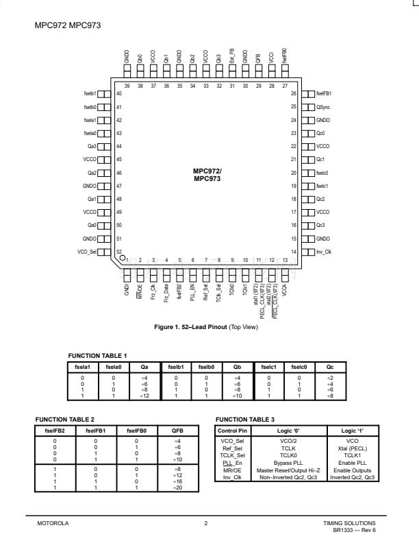
The MPC972/973 features an extensive level of frequency
programmability between the 12 outputs as well as the input vs output
relationships. Using the select lines output frequency ratios of 1:1, 2:1,
3:1, 3:2, 4:1, 4:3, 5:1, 5:2, 5:3, 6:1 and 6:5 between outputs can be
realized by pulsing low one clock edge prior to the coincident edges of the
Qa and Qc outputs. The Sync output will indicate when the coincident
rising edges of the above relationships will occur. The selectability of the
feedback frequency is independent of the output frequencies, this allows
for very flexible programming of the input reference vs output frequency
relationship. The output frequencies can be either odd or even multiples
of the input reference. In addition the output frequency can be less than
the input frequency for applications where a frequency needs to be
reduced by a non鈥揵inary factor. The Power鈥揙n Reset ensures proper
programming if the frequency select pins are set at power up. If the
fselFB2 pin is held high, it may be necessary to apply a reset after
power鈥搖p to ensure synchronization between the QFB output and the
other outputs. The internal power鈥搊n reset is designed to provide this
function, but with power鈥搖p conditions being system dependent, it is
difficult to guarantee. All other conditions of the fsel pins will automatically
synchronize during PLL lock acquisition.
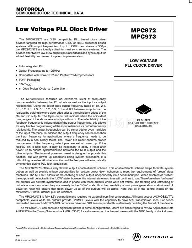
FA SUFFIX
52鈥揕EAD TQFP PACKAGE
CASE 848D-03
The MPC972/973 offers a very flexible output enable/disable scheme. This enable/disable scheme helps facilitate system
debug as well as provide unique opportunities for system power down schemes to meet the requirements of 鈥済reen鈥?class
machines. The MPC972 allows for the enabling of each output independently via a serial input port. When disabled or 鈥渇rozen鈥?/div>
the outputs will be locked in the 鈥淟OW鈥?state, however the internal state machines will continue to run. Therefore when 鈥渦nfrozen鈥?/div>
the outputs will activate synchronous and in phase with those outputs which were not frozen. The freezing and unfreezing of
outputs occurs only when they are already in the 鈥淟OW鈥?state, thus the possibility of runt pulse generation is eliminated. A
power-on reset will ensure that upon power up all of the outputs will be active. Note that all of the control inputs on the
MPC972/973 have internal pull鈥搖p resistors.
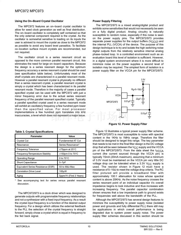
The MPC972/973 is fully 3.3V compatible and requires no external loop filter components. All inputs accept LVCMOS/LVTTL
compatible levels while the outputs provide LVCMOS levels with the capability to drive 50鈩?transmission lines. For series
terminated lines each MPC972/973 output can drive two 50鈩?lines in parallel thus effectively doubling the fanout of the device.
The MPC972/973 can consume significant power in some configurations. Users are encouraged to review Application Note
AN1545/D in the Timing Solutions book (BR1333/D) for a discussion on the thermal issues with the MPC family of clock drivers.
PowerPC is a trademark of International Business Machines Corporation. Pentium is a trademark of Intel Corporation.
8/97
漏
Motorola, Inc. 1997
1
REV 1


 1
1
 2
2
 3
3
 4
4
 5
5
 6
6
 7
7
 8
8
 9
9
 10
10
 11
11
 12
12
 13
13
 14
14
