N Suffix Indicates Lead - Free Terminations. RoHS Compliant.
鈥?/div>
In Tape and Reel. R1 Suffix = 500 Units per 44 mm, 13 inch Reel.
V
RD2
V
RG2
V
DS1
MWIC930NR1
MWIC930GNR1
746 - 960 MHz, 30 W, 26 - 28 V
SINGLE N - CDMA, GSM/GSM EDGE
RF LDMOS WIDEBAND INTEGRATED
POWER AMPLIFIERS
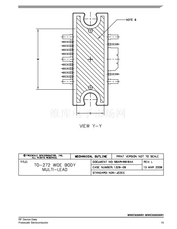
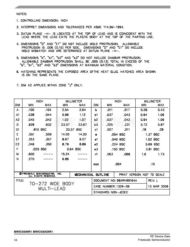
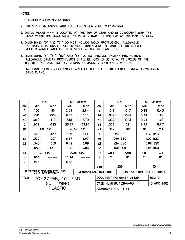
CASE 1329 - 09
TO - 272 WB - 16
PLASTIC
MWIC930NR1
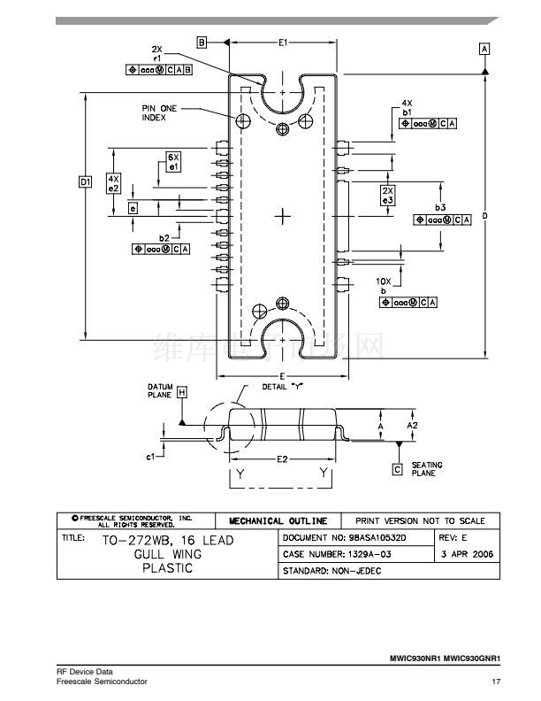
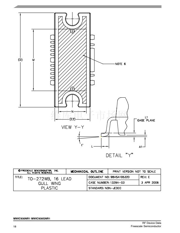
CASE 1329A - 03
TO - 272 WB - 16 GULL
PLASTIC
MWIC930GNR1
GND
V
RD2
V
RG2
V
DS1
V
RD1
V
DS2
/RF
out
RF
in
V
RG1
V
GS1
V
GS2
NC
GND
1
2
3
4
5
6
7
8
9
10
11
16
15
GND
NC
14
RF
in
V
RD1
V
RG1
RF
out/
V
DS2
13
12
NC
GND
V
GS1
V
GS2
Quiescent Current
Temperature Compensation
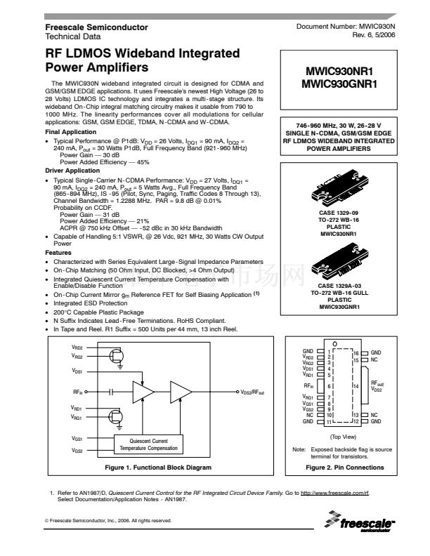
(Top View)
Note: Exposed backside flag is source
terminal for transistors.
Figure 1. Functional Block Diagram
Figure 2. Pin Connections
1. Refer to AN1987/D,
Quiescent Current Control for the RF Integrated Circuit Device Family.
Go to http://www.freescale.com/rf.
Select Documentation/Application Notes - AN1987.
漏
Freescale Semiconductor, Inc., 2006. All rights reserved.
MWIC930NR1 MWIC930GNR1
1
RF Device Data
Freescale Semiconductor


 1
1
 2
2
 3
3
 4
4
 5
5
 6
6
 7
7
 8
8
 9
9
 10
10
 11
11
 12
12
 13
13
 14
14
 15
15
 16
16
 17
17
 18
18
 19
19
 20
20
