鈫?/div>
PIC16F72 Migration
DEVICE MIGRATIONS
This document is intended to describe the differences that are present when migrating from one device to the next.
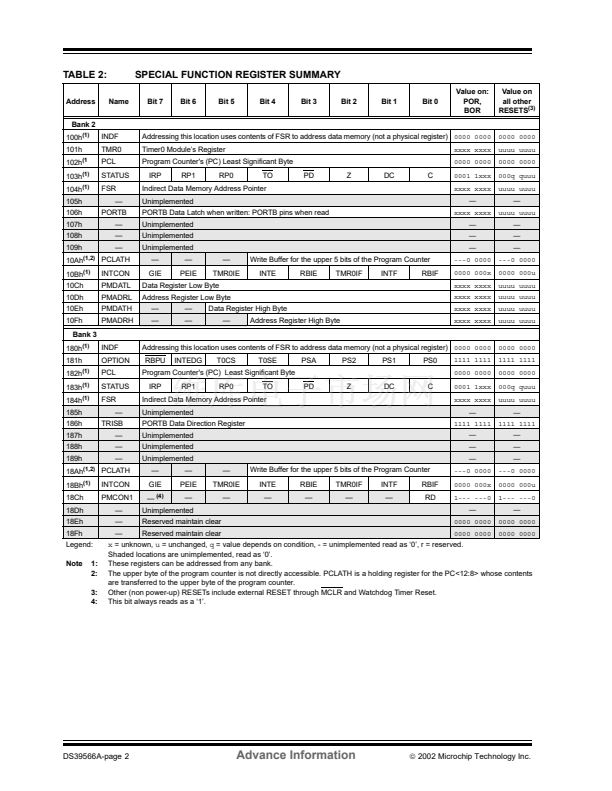
Table 1 and Table 2 list the data memory organization differences and the additional Special Function Registers, Table 3
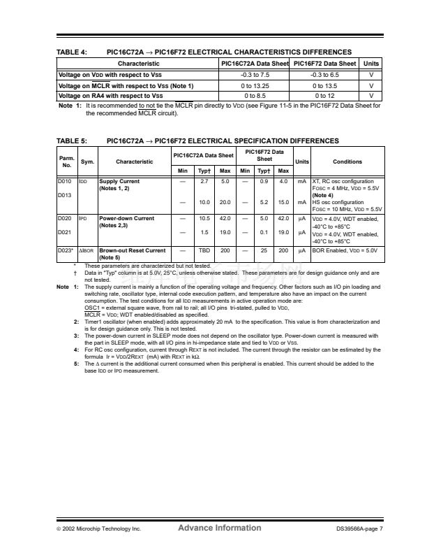
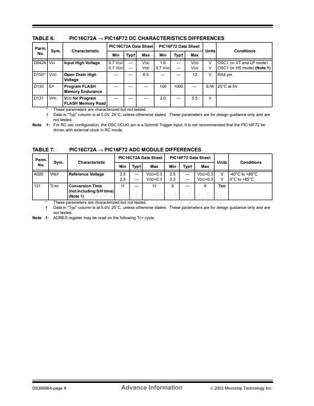
lists the differences in functionality, and Table 4 through Table 7 list the differences in the electrical and timing specifi-
cations.
This device has been designed to perform to the parameters of its data sheet. It has been tested to an elec-
trical specification designed to determine its conformance with these parameters. Due to process differ-
ences in the manufacture of this device, this device may have different performance characteristics than its
earlier version. These differences may cause this device to perform differently in your application than the
earlier version of this device.
Note:
The user should verify that the device oscillator starts and performs as expected. Adjusting the loading
capacitor values and/or the oscillator mode may be required.
TABLE 1:
No.
1
2
3
4
5
6
7
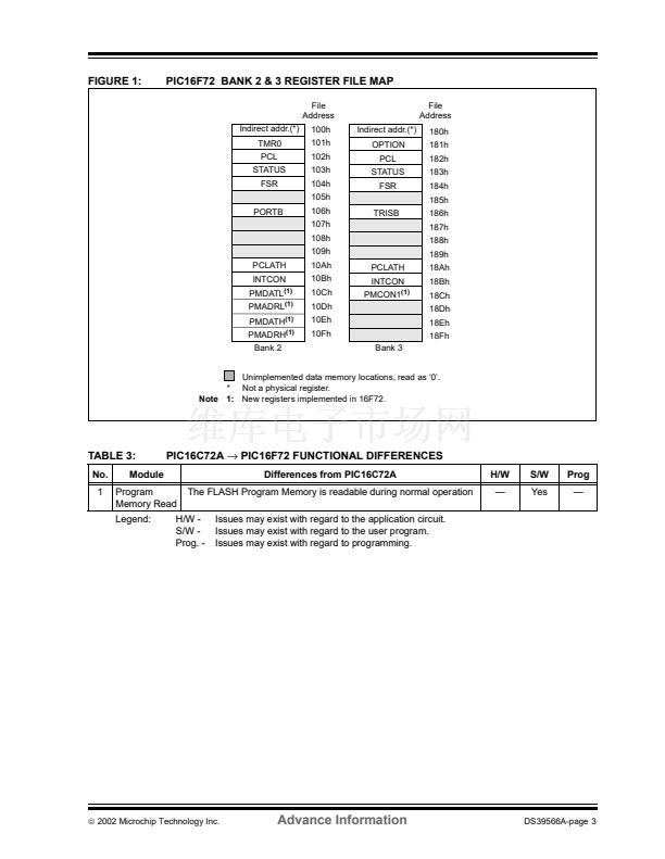
BANK 2
BANK 3
PIC16C72A
鈫?/div>
PIC16F72 DATA MEMORY DIFFERENCES
SFR
Differences from PIC16C72A
BANK 2 is implemented
BANK 3 is implemented
Implemented
Implemented
Implemented
Bit 6 (RP1) and Bit 7 (IRP) are implemented
Bit 2 (TMR0IF) and Bit 5 (TMR0IE)
Address register pair
Data register pair
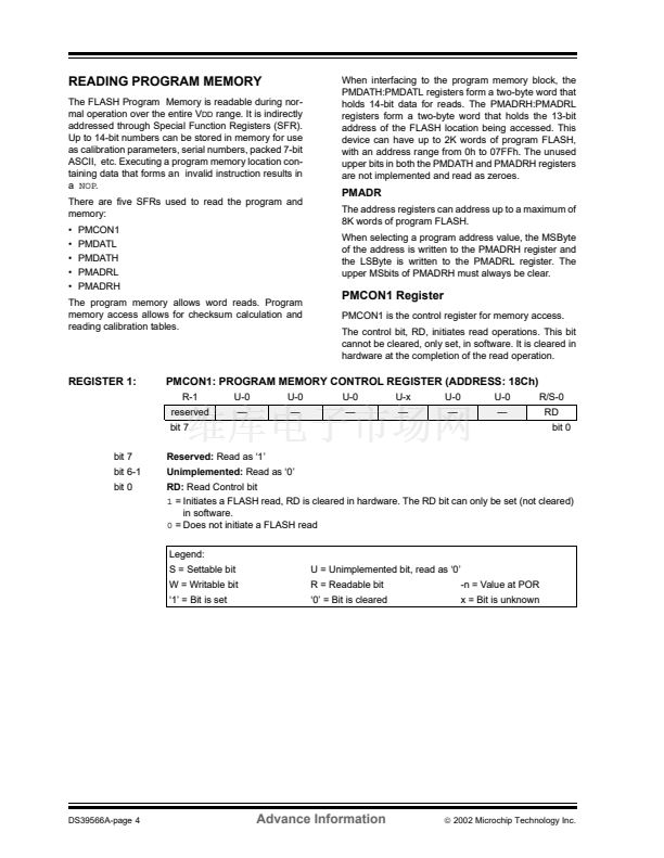
Control register for memory access
RP1 to access BANK 2 & 3,
IRP used for indirect addressing
T0IF and T0IE in PIC16C72A
Comment
PMADRH:PMADRL
PMDATH:PMDATL
PMCON1
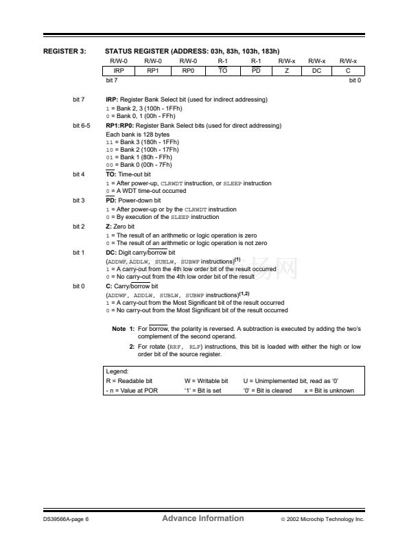
STATUS
INTCON
铮?/div>
2002 Microchip Technology Inc.
Advance Information
DS39566A-page 1


 1
1
 2
2
 3
3
 4
4
 5
5
 6
6
 7
7
 8
8
 9
9
 10
10
