鈮?/div>
1 V
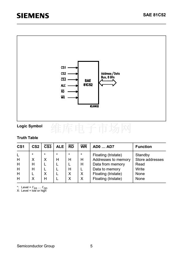
Three different chip select inputs for two chip
select modes
No increasing power consumption in standby mode
if the control inputs are on undefined potential
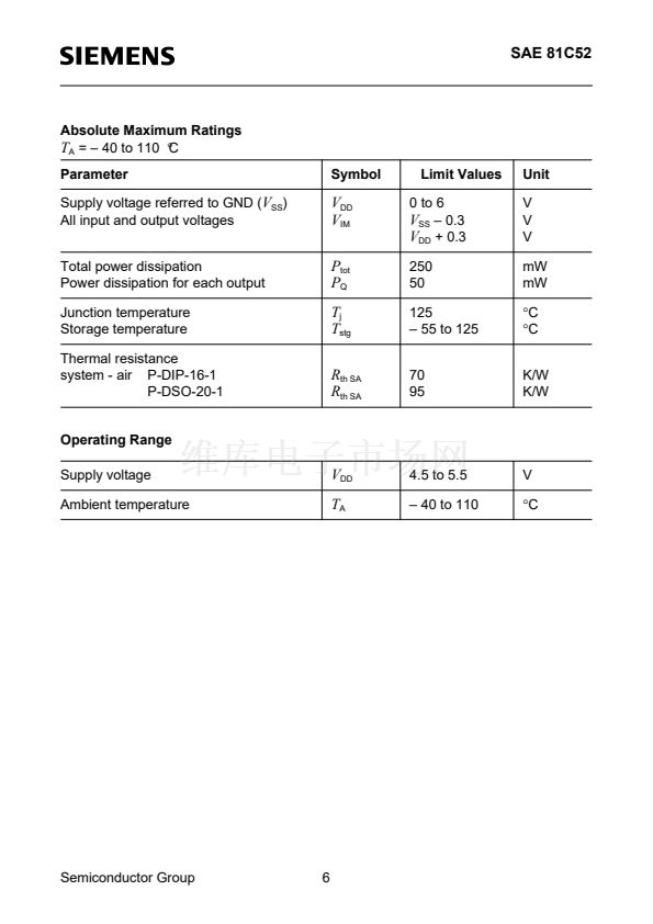
Temperature range 鈥?40 to 110
掳C
P-DIP-16-1
P-DSO-20-1
Type
SAE 81C52 P
SAE 81C52 G
Ordering Code
Q67100-H9017
Q67100-H9015
Package
P-DIP-16-1
P-DSO-20-1 (SMD)
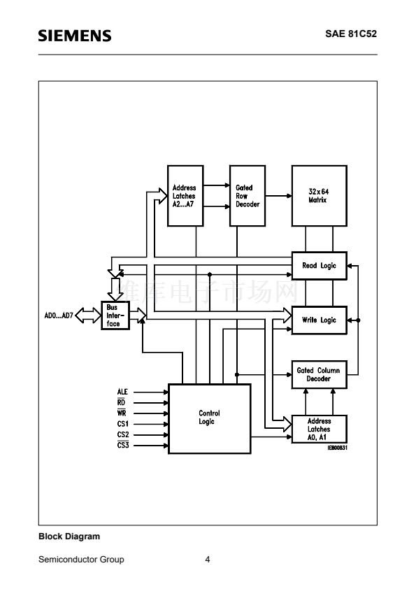
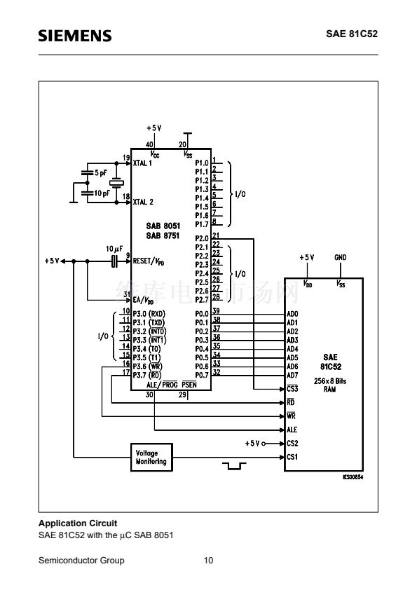
The SAE 81C52 is a CMOS-silicon gate, static random access memory (RAM),
organized as 256 words by 8 bits. The multiplexed address and data bus interfaces
directly to 8-bit microprocessors/microcontrollers without any timing or level problems,
e.g. the families SAB 8086, SAB 8051.
All inputs and outputs are fully compatible with NMOS circuits, except CS1. Data
retention is ensured up to
V
DD
鈮?/div>
1.0 V. The SAE 81C52 has three different inputs for two
chip select modes which allow to inhibit either the address/data lines (AD 0 鈥?AD 7) and
the control lines (WR, RD, ALE, CS2, CS3), or only the control lines RD, WR.
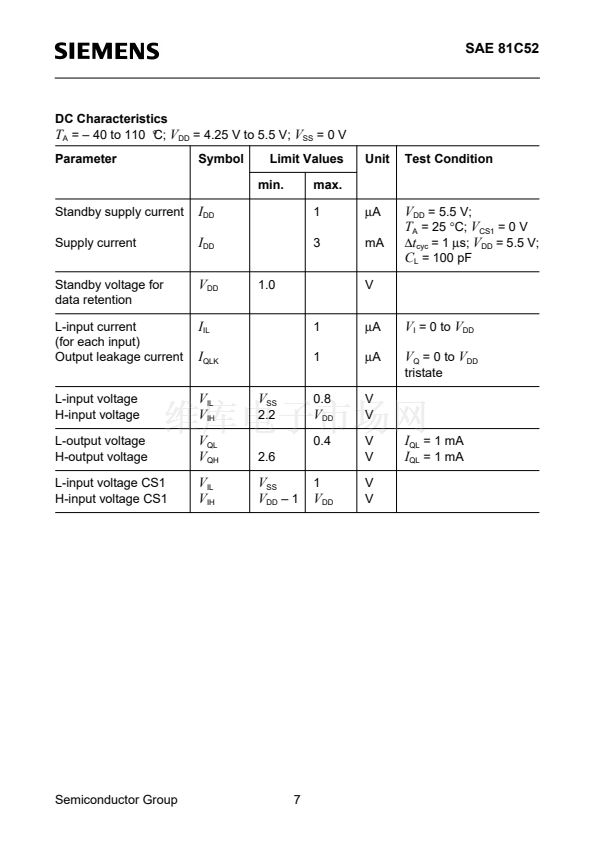
The power consumption is max. 5.5
碌W
in standby mode and max. 16.5 mW in
operation. In standby mode, the power consumption will not increase if the control inputs
are on undefined potential.
Semiconductor Group
1
09.94


 1
1
 2
2
 3
3
 4
4
 5
5
 6
6
 7
7
 8
8
 9
9
 10
10
