鈥?/div>
Synchronous Buck Controller (VDDQ)
鈥?Wide-Input Voltage Range: 3.0-V to 28-V
鈥?D鈥揅AP鈩?Mode with 100-ns Load Step Re-
sponse
鈥?Current Mode Option Supports Ceramic
Output Capacitors
鈥?Supports Soft-Off in S4/S5 States
鈥?Current Sensing from R
DS(on)
or Resistor
鈥?2.5-V (DDR), 1.8-V (DDR2) or Adjustable
Output (1.5-V to 3.0-V)
鈥?Equipped with Powergood, Overvoltage Pro-
tection and Undervoltage Protection
3-A LDO (VTT), Buffered Reference (VREF)
鈥?Capable to Sink and Source 3 A
鈥?LDO Input Available to Optimize Power
Losses
鈥?Requires only 20-碌F Ceramic Output Ca-
pacitor
鈥?Buffered Low Noise 10-mA Output
鈥?Accuracy
卤20
mV for both VREF and VTT
鈥?Supports High-Z in S3 and Soft-Off in S4/S5
鈥?Thermal Shutdown
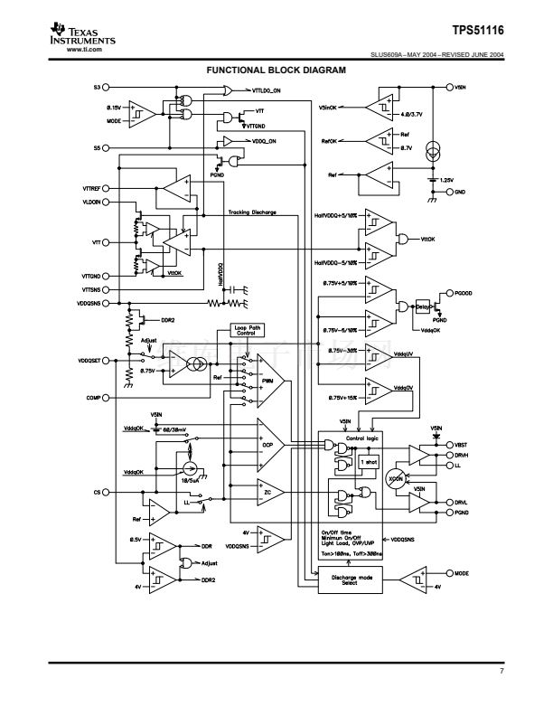
DESCRIPTION
The TPS51116 provides a complete power supply for
both DDR/SSTL-2 and DDR2/SSTL-18 memory sys-
tems. It integrates a synchronous buck controller with
a 3-A sink/source tracking linear regulator and
buffered low noise reference. The TPS51116 offers
the lowest total solution cost in systems where space
is at a premium. The TPS51116 synchronous control-
ler runs fixed 400kHz pseudo-constant frequency
PWM with an adaptive on-time control that can be
configured in D-CAP鈩?Mode for ease of use and
fastest transient response or in current mode to
support ceramic output capacitors. The 3-A
sink/source LDO maintains fast transient response
only requiring 20-碌F (2
脳
10 碌F) of ceramic output
capacitance. In addition, the LDO supply input is
available externally to significantly reduce the total
power losses. The TPS51116 supports all of the
sleep state controls placing VTT at high-Z in S3
(suspend to RAM) and discharging VDDQ, VTT and
VTTREF (soft-off) in S4/S5 (suspend to disk). The
TPS51116 has all of the protection features including
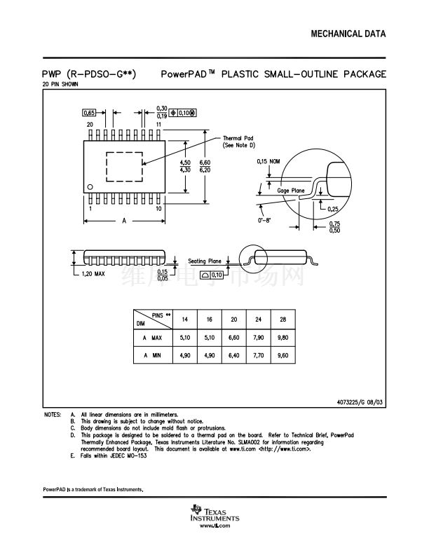
thermal shutdown and is in a 20-pin HTSSOP
PowerPAD鈩?package.
鈥?/div>
APPLICATIONS
鈥?/div>
鈥?/div>
DDR/DDR2 Memory Power Supplies
SSTL-2 SSTL-18 and HSTL Termination
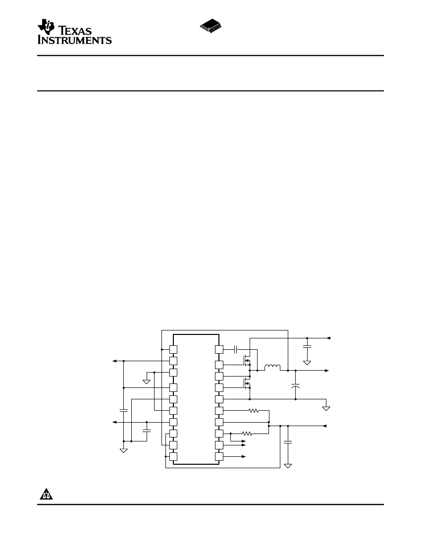
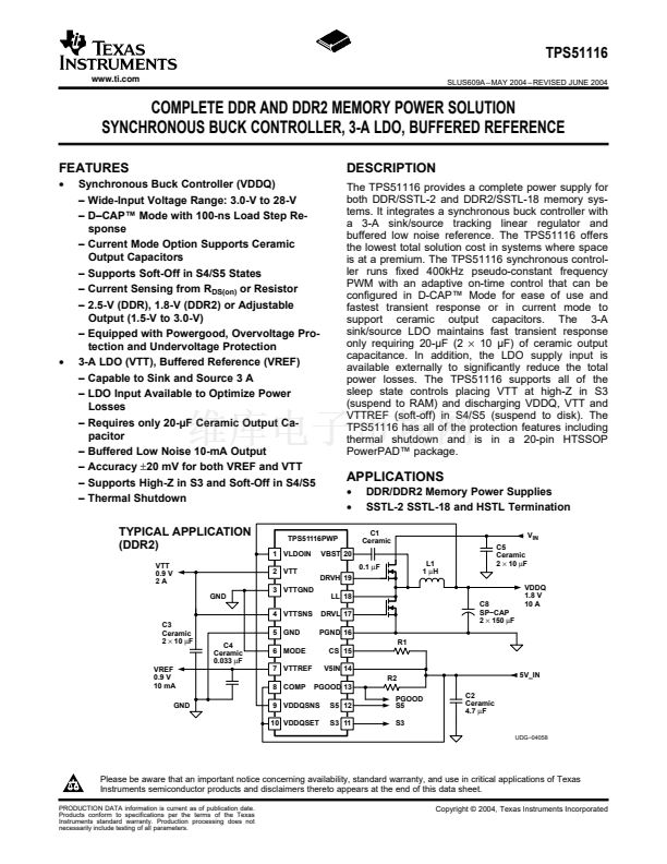
C1
Ceramic
0.1
碌F
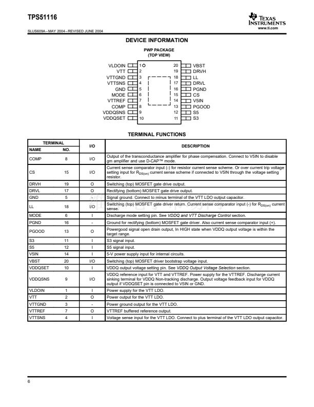
DRVH 19
LL 18
DRVL 17
C8
SP鈭扖AP
2
脳
150
碌F
R1
L1
1
碌H
V
IN
C5
Ceramic
2
脳
10
碌F
VDDQ
1.8 V
10 A
TYPICAL APPLICATION
(DDR2)
VTT
0.9 V
2A
GND
TPS51116PWP
1 VLDOIN
2 VTT
3 VTTGND
4 VTTSNS
VBST 20
C3
Ceramic
2
脳
10
碌F
5 GND
C4
Ceramic
0.033
碌F
6 MODE
7 VTTREF
8 COMP
PGND 16
CS 15
V5IN 14
R2
PGOOD 13
S5 12
S3 11
PGOOD
S5
S3
UDG鈭?4058
VREF
0.9 V
10 mA
GND
5V_IN
C2
Ceramic
4.7
碌F
9 VDDQSNS
10 VDDQSET
Please be aware that an important notice concerning availability, standard warranty, and use in critical applications of Texas
Instruments semiconductor products and disclaimers thereto appears at the end of this data sheet.
PRODUCTION DATA information is current as of publication date.
Products conform to specifications per the terms of the Texas
Instruments standard warranty. Production processing does not
necessarily include testing of all parameters.
Copyright 漏 2004, Texas Instruments Incorporated


 1
1
 2
2
 3
3
 4
4
 5
5
 6
6
 7
7
 8
8
 9
9
 10
10
 11
11
 12
12
 13
13
 14
14
 15
15
 16
16
 17
17
 18
18
 19
19
 20
20
 21
21
 22
22
 23
23
 24
24
 25
25
 26
26
 27
27
 28
28
 29
29
