|
|||||||||||
| �������� | ��·���� | ������� | ���ֹ�� | ͨ�ż��� | ��Դ���� | ���֮�� | EMC���� | ARM���� | EDA���� | PCB���� | Ƕ��ʽϵͳ ������� | ���ɵ�· | �����滻 | ģ�⼼�� | ������ | �� Ƭ �� | DSP���� | MCU���� | IC ��� | IC ��ҵ | CAN-bus/DeviceNe |
���ַ��룺TI���������ֲ�������ŵĽ��������� |
||||
| ���ߣ�kasami����Ŀ��ģ�⼼�� | ||||
��ƪ���¶��Ķ����Ϻ��òο���ֵ�����ע��
ԭ����Stephen M. Nolan and JOSE M. Soltero ���룺kasami ABSTRACT ժҪ
˵��������һλ���ѵĽ��飬��������ѧϰ��̬����������ƪ���£����Ҷ�ӵ��������ָ�̡���Ҫ����½���ǣ���û�б������ӣ���Ҫԭ�ģ��뵽TI��վ���ң�Ҳ�������ҵ������Ѹ����ṩ���ӣ�ѧ���ڴ���л������ˣ��� * - ���������ʱ�䣺2005-4-24 0:41:35 ���ߣ�IC921 |
| 2¥�� | >>�������� |
| ���ߣ� IC921 �� 2005/4/13 22:38:00 ������
kasamiͬѧ���룬���Ҵ���֧�֣��� kasamiͬѧ���룬���Ҵ���֧�֣��� |
|
| 3¥�� | >>�������� | |||||||||||||||||||||||||||||||||||||||||||||||||||||||||||||||||||||||||||
| ���ߣ� IC921 �� 2005/4/13 22:45:00 ������
��ͼ���Ӻ������Ƽ�
* - ���������ʱ�䣺2005-4-24 21:57:53 ���ߣ�IC921 |
||||||||||||||||||||||||||||||||||||||||||||||||||||||||||||||||||||||||||||
 ������.jpg
 ������.jpg (854)
 ������.jpg (869)
 ���Ƿ���.jpg (890)
| 4¥�� | >>�������� |
| ���ߣ� akaer �� 2005/4/13 22:52:00 ������
Thanks, kasami! �о��������������������ԭ��ͦ���ġ��������һ�βμ����ַ�������������˹淶��ʵ���ѵã� ��һ���У���һ���ط�����̽�֣�electrical specifications���Ҿ��÷���ɡ�����ָ�ꡱ����Щ�� �ڴ���������Ʒ�� * - ���������ʱ�䣺2005-4-13 23:01:02 ���ߣ�akaer |
|
| 5¥�� | >>�������� |
| ���ߣ� IC921 �� 2005/4/13 23:07:00 ������
�ļ�Ŀ¼(����Ϊ�ֽ�֮�ο�) ��ͼ�б� 2 ABSTRACT ժҪ 3 ����Ŀ¼ 4 1 Introduction ���� 7 2 Top-Level Look at the TI LOGIC Data Sheet 7 2.1 Summary DEVICE DESCRIPTION 8 2.2 Absolute Maximum Ratings 10 2.3 Recommended Operating Conditions �Ƽ��������� 11 2.4 Electrical Characteristics 13 2.5 Live-Insertion Specifications 14 2.6 Timing Requirements 15 2.7 Switching Characteristics 16 2.8 Noise Characteristics 17 2.9 Operating Characteristics 17 2.10 Parameter Measurement Information 18 3 Dissecting the TI LOGIC Data Sheet 19 3.1 Summary DEVICE DESCRIPTION 20 3.1.1 Title, Literature NUMBER, and Dates of Origination and Revision 20 3.1.1.1 Example: 20 3.1.1.2 Level-Shifting DIODE (D) 24 3.1.1.3 Bus-Hold (H) 25 3.1.1.4 Damping RESISTOR on Inputs/OUTPUTs (R) 26 3.1.1.5 Schottky Clamping DIODE (S) 26 3.1.1.6 Undershoot-Protection Circuitry (K) 27 3.1.1.7 Power-Up 3-State (Z) 28 3.1.2 Features Bullets 29 3.1.3 PACKAGE Options and Pinouts 30 3.1.4 DESCRIPTION 31 3.1.5 BGA Packaging Top-View Illustrations and Pin-Assignments Table 31 3.1.6 Ordering Information 31 3.1.7 Function Table 33 3.1.8 LOGIC Diagram 36 3.1.9 PRODUCT Development Stage Note 37 3.2 Absolute Maximum Ratings 38 3.2.1 Supply Voltage, VCC 38 3.2.2 Input Voltage, VI 38 3.2.3 OUTPUT Voltage, VO 39 3.2.4 Voltage Range Applied to Any OUTPUT in the High-Impedance or Power-Off State, VO 40 3.2.5 Voltage Range Applied to Any OUTPUT in the High State, VO 41 3.2.6 Input Clamp Current, IIK 41 3.2.7 OUTPUT Clamp Current, IOK 42 3.2.8 Continuous OUTPUT Current, IO 42 3.2.9 Continuous Current Through VCC or GND Terminals 42 3.2.10 PACKAGE THERMAL Impedance, Junction-to-Ambient, ��JA 42 3.2.11 Storage Temperature Range, Tstg 43 3.3 Recommended Operating Conditions �Ƽ��������� 43 3.3.1 VCC Supply Voltage 43 3.3.2 BIAS VCC Bias Supply Voltage 44 3.3.3 VTT Termination Voltage 44 3.3.4 Vref Reference Voltage 45 3.3.5 VIH High-Level Input Voltage 45 3.3.6 VIL Low-level Input Voltage 47 3.3.7 IOH High-Level OUTPUT Current 49 3.3.8 IOHS Static High-Level OUTPUT Current 49 3.3.9 IOL Low-Level OUTPUT Current 50 3.3.10 IOLS Static Low-Level OUTPUT Current 51 3.3.11 VI Input Voltage 52 3.3.12 VO OUTPUT Voltage 53 3.3.13 ��t /��v Input Transition Rise or Fall Rate 54 3.3.14 ��t /��VCC Power-up Ramp Rate 55 3.3.15 TA Operating Free-Air Temperature 55 3.4 Electrical Characteristics 59 3.4.1 VT+ Positive-Going Input Threshold Level 59 3.4.2 VT�C Negative-Going Input Threshold Level 60 3.4.3 ��VT Hysteresis (VT+ �C VT�C) 60 3.4.4 VIK Input Clamp Voltage 63 3.4.5 VOH High-Level OUTPUT Voltage 63 3.4.6 VOHS Static High-level OUTPUT Voltage 64 3.4.7 VOL Low-Level OUTPUT Voltage 65 3.4.8 VOLS Static Low-Level OUTPUT Voltage 65 3.4.9 ron On-State Resistance 66 3.4.10 II Input Current 66 3.4.11 IIH High-Level Input Current 67 3.4.12 IIL Low-Level Input Current 68 3.4.13 II(hold) Input Hold Current 68 3.4.13 IBHH Bus-Hold High Sustaining Current 70 3.4.14 IBHL Bus-Hold Low Sustaining Current 71 3.4.15 IBHHO Bus-Hold High Overdrive Current 71 3.4.16 IBHLO Bus-Hold Low Overdrive Current 71 3.4.17 Ioff Input/OUTPUT Power-Off Leakage Current 72 3.4.18 IOZ Off-State (High-Impedance State) OUTPUT Current (of a 3-State OUTPUT) 74 3.4.19 IOZH Off-State OUTPUT Current With High-Level Voltage Applied 75 3.4.20 IOZL Off-State OUTPUT Current With Low-Level Voltage Applied 76 3.4.21 IOZPD Power-Down Off-State (High-Impedance State) OUTPUT Current (of a 3-State OUTPUT) 77 3.4.22 IOZPU Power-Up Off-State (High-Impedance State) OUTPUT Current (of a 3-State OUTPUT) 79 3.4.23 ICEX OUTPUT High Leakage Current 79 3.4.24 ICC Supply Current 80 3.4.25 ��ICC Supply-Current Change 80 3.4.26 Ci Input Capacitance 81 3.4.27 Cio Input/OUTPUT Capacitance 82 3.4.29 Co OUTPUT Capacitance 83 3.5 Live-Insertion Specifications 83 3.5.1 ICC (BIAS VCC) BIAS VCC Current 83 3.5.2 VO OUTPUT Bias Voltage 84 3.5.3 IO OUTPUT Bias Current 84 3.6 Timing Requirements 84 3.6.1 fclock Clock Frequency 84 3.6.2 tw PULSE Duration (Width) 85 3.6.3 tsu Setup Time 86 3.6.4 th Hold Time 87 3.7 Switching Characteristics 89 3.7.1 fmax Maximum Clock Frequency 89 3.7.2 tpd Propagation Delay Time 90 3.7.3 tPHL Propagation Delay Time, High-Level to Low-Level OUTPUT 91 3.7.4 tPLH Propagation Delay Time, Low-Level to High-Level OUTPUT 92 3.7.5 ten Enable Time (of a 3-State or Open-Collector OUTPUT) 93 3.7.6 tPZH Enable Time (of a 3-State OUTPUT) to High Level 93 3.7.8 tPZL Enable Time (of a 3-State OUTPUT) to Low Level 94 3.7.9 tdis Disable Time (of a 3-State or Open-Collector OUTPUT) 95 3.7.10 tPHZ Disable Time (of a 3-State OUTPUT) From High Level 95 3.7.11 tPLZ Disable Time (of a 3-State OUTPUT) From Low Level 96 3.7.12 tf Fall Time 96 3.7.13 tr Rise Time 96 3.7.14 Slew Rate 97 3.7.15 tsk(i) Input Skew 97 3.7.16 tsk(l) Limit Skew 97 3.7.17 tsk(o) OUTPUT Skew 98 3.7.18 tsk(p) PULSE Skew 98 3.7.19 tsk(pr) PROCESS Skew 99 3.8 Noise Characterist |
|
| 6¥�� | >>�������� | ||||||||||||
| ���ߣ� kasami �� 2005/4/13 23:48:00 ������
TI�������·��룺���������ֲ�������ŵĽ��������� ��2�� Introduction ����
Top-Level Look at the TI LOGIC Data Sheet
* - ���������ʱ�䣺2005-4-15 0:13:02 ���ߣ�IC921 |
|||||||||||||
| 7¥�� | >>�������� |
| ���ߣ� IC921 �� 2005/4/14 1:41:00 ������
��003��2.Top-Level Look at the TI Data Sheet ���ݹۡ�һ�ʽ����Ϊ����ò���� ͬһ�䣺component parts of a data sheet ���������ֲ����ɲ��֡����á� ��002�ݵȴ���componentһ�ʣ��о����ã���һʱ�Ҳ������ʵĴ������ |
|
| 8¥�� | >>�������� |
| ���ߣ� kenand �� 2005/4/14 8:24:00 ������
to kasami abstrct ................ abstract................ ������������ı���, |
|
| 9¥�� | >>�������� |
| ���ߣ� kasami �� 2005/4/14 11:35:00 ������
��Ц�ˣ���ȷ�DZ��� |
|
| 10¥�� | >>�������� |
| ���ߣ� kasami �� 2005/4/14 11:37:00 ������
лл���һ����Ŭ���ģ��������� |
|
| 11¥�� | >>�������� |
| ���ߣ� kasami �� 2005/4/14 11:44:00 ������
��л��λ ��л��λ�ı�����������˵�һ�η��룬�в���֮��������ָ�̣�лл�� |
|
| 12¥�� | >>�������� |
| ���ߣ� kasami �� 2005/4/14 11:49:00 ������
electrical specifications ������ָ�ꡱ���� |
|
| 13¥�� | >>�������� |
| ���ߣ� kasami �� 2005/4/14 12:05:00 ������
����ô���벻���أ� Top-Level Look ����ɡ���ò�� ������̫�����ˣ�����ô���벻���أ���� |
|
| 14¥�� | >>�������� |
| ���ߣ� ����ɴ� �� 2005/4/14 15:16:00 ������
organized into five main sections��仰���뷨�г��룿 This application report is organized into five main sections: ���Ӧ�ñ����������������֣� //------------------------------------------- ��仰�����ɣ���Ӧ�ñ�������Ҫ�����������ɡ� ���ܸ�����ԭ������˼�� organized into ���ɡ�����������������˼ main sections ���е�main ������ five section.����Ҫ�����ݴ����β��ֵ���˼Ҳȷ���������������֮���� |
|
| 15¥�� | >>�������� |
| ���ߣ� zhousd �� 2005/4/14 16:40:00 ������
very GOOD! |
|
| 16¥�� | >>�������� |
| ���ߣ� kasami �� 2005/4/14 16:41:00 ������
Ϊʲô����ɣ����Ӧ�ñ����������Ҫ������� ��This application report is organized into five main sections:����ɡ����Ӧ�ñ����������Ҫ������ɣ������Ǹ�����ԭ����˼�� |
|
| 17¥�� | >>�������� |
| ���ߣ� zhousd �� 2005/4/14 16:52:00 ������
��Ž�ˮƽ������ɴ���Ȼ������ ���������ѣ�һ�����֣���������ľ���֣���Ž�E��ˮƽ�� ��˵¥�ϵ�kasami ����ͬTI �����ɣ�����ķ�������û��һ��ʵ����������ˮƽ������˼�ڴ˰ڡ� ʲô����E ��ˮƽ��֪���𣿺õķ������¾���һ���ֳɵ���̲ģ� ����ɴ�������������Ǿ�ͽ�ˮƽ��������ǰ������Ҳ�� * - ���������ʱ�䣺2005-4-14 17:01:48 ���ߣ�zhousd |
|
| 18¥�� | >>�������� |
| ���ߣ� akaer �� 2005/4/14 18:53:00 ������
��zhousd�ļ������⻰ ���ѵ����ۣ��������������ǹ�����ֻҪ�����۵㣬��Ϊ���ַ����IJ����ߣ����Ŷ�����Ϊ�Ƕ��Լ�Ŭ���Ͷ������÷����� �������Ҿ�������������һ��������̳��kasami�����Լ��ܶ�����߶�����ѧϰ������������ǰ���£������ַ�ʽ����Ӣ����������ˣ�����Ϊ���š���ŵ���Ҫ���£��Dz��ǿ���������һ�£������š�������š����ܸ���ʵЩ����˵�أ����� |
|
| 19¥�� | >>�������� |
| ���ߣ� IC921 �� 2005/4/14 19:20:00 ������
to zhousd��лл�������ͣ���Ҫע��һ��ԭ�� ���ó���dz�����ɴ�������! ������˵����һ���ǣ�kasami����ѧ��������ƪ����ԭ���Dz�ȡ�ҵĽ���Ľ������Ҫ����ˡ��ϸ�һ���˵����TI�����Ҳ�������ο�Ʋ��TI���Ļ���˵����TI������Ҳ�����룬�������̳��Ҳ��û��ʲô��˼�ˡ�kasamiͬѧ���ڳ�������������ĥ���Լ�������dz��ɿɼΣ�Ҫ��������ָ������Ҫ�Ը����Ͷ�������ˮƽ�����ʵ������ۻ����ѣ������˺����䱾���������˵Ļ����ԡ����ԭ��Ӧ�����պá� ��ƪ���·dz���������ȫ���˽⣬�������Ķ����Ϸdz��а��������������䱾�����������˶Թ��ʻ���˾�Ĺ淶���������ܣ�������ƪ�����ѵõĵط�֮һ�� ����ʵ�����ݻ��ں��棬������شӼ��������ϼ���֧�֡����룬������������TI��ADI�ȹ�����Ƶ����£������Ǹ��ɴ����ͣ�����õ�����Ļ�ӭ�� |
|
| 20¥�� | >>�������� |
| ���ߣ� kasami �� 2005/4/14 19:43:00 ������
thanks ,akaer and IC921 |
|
| 21¥�� | >>�������� |
| ���ߣ� asunmad �� 2005/4/14 21:02:00 ������
֧��һ�£�˳������һ�¡� ����������ij����Ʒ��DATA SHEET���й��֮�ӵĻ����������ָ����ԵIJ���Ӧ��˵��һ��ֵ���ᳫ����Ϊ����ʵ�������������ݲ�������ֻ��������ijһ�ҹ�˾�IJ�Ʒ��Ū�������������Ķ��κ�һ�ҹ�˾ͬ���Ʒ��DATA SHEET�����а����ġ� �ͷ���η���ò�����ֵ��ѧϰ���������Ļ���˵�����������ֱ�ʾ֧�ְ�~~~ [002] To assist component and system-design engineers in selecting Texas Instruments (TI) standard-logic products, this application report is a synopsis of the information available from a typical TI data sheet. Ϊ���������ϵͳ��ƹ���ʦѡ��TI������Ʒ�����Ӧ�ñ����������ڵ���TI���ݲ��������Ϣ��ժҪ�� ��˼��ȷ�����������Ըб�Ť���þ俪ͷ��To=In order to��������״��Ӿ�ɷ�һ����ǰ�棬Ҳ���Էŵ�������档�Ҹо�������ŵ�����������������Щ��������ķ���������ȥ�����벻�ã��������£� ���Ӧ�ñ����ǶԵ��͵�TI�����ֲ������ṩ����Ϣ��һ��ժҪ��Ŀ����Ϊ�˰��������ƹ���ʦ��ϵͳ��ƹ���ʦѡ��TI�ı�����Ʒ�� Symbols, terms, and definitions generally are in accordance with those currently agreed upon by the JEDEC Solid State TECHNOLOGY Association for use in the USA and by the International Electrotechnical Commission (IEC) for international use. ���š�����Ͷ���һ����JEDEC��IEC����������Э���йء� in accordance with���롭��һ�µ���˼�����ǡ��йء������룺 �������У����š��������һ����JEDEC��̬����Э���Ͽ�����������ʹ�õķ��š���������Լ����ʵ繤ίԱ�ᣨIEC���Ͽ��ڹ�����ʹ�õķ��š����������һ�µġ� �о��ҵ������е��߳���ϣ�����˰��Ҽ�����:) * - ���������ʱ�䣺2005-4-14 21:06:02 ���ߣ�asunmad |
|
| 22¥�� | >>�������� |
| ���ߣ� ����ɴ� �� 2005/4/14 22:45:00 ������
to zhousd �ϸ�����������ƽ��һ��ͺ� ����һƪ����רҵ�������²����ף�Ҫ�����ܴ��Ŭ���;�����������ÿ�䶼����ú�ȷ�Ǻ��ѵ��£�kasami ������������Ѿ��ܲ����ˣ������ʻ�û���ﵽ�����ˮƽ������������ˮƽ�ܸ߰ɣ���Ҳ��������������̬�Դ����ˡ�����Ӧ��Ϊ�������������Ŷԣ������������Ŀ����� ̳���¿��ţ���Ҫ��ҺõĽ���Ͳ��룬ϣ���������һ�й��ǣ������ػ��� * - ���������ʱ�䣺2005-4-14 23:08:41 ���ߣ�����ɴ� |
|
| 23¥�� | >>�������� | ||||||||
| ���ߣ� kasami �� 2005/4/14 23:51:00 ������
TI�������·��룺���������ֲ�������ŵĽ���������(3) Summary DEVICE DESCRIPTION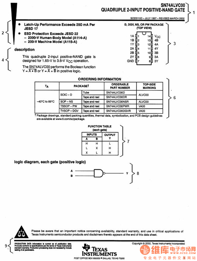 Figure 1. Example of Summary DEVICE DESCRIPTION
* - ���������ʱ�䣺2005-4-15 0:24:58 ���ߣ�IC921 |
|||||||||
| 24¥�� | >>�������� |
| ���ߣ� kasami �� 2005/4/15 13:04:00 ������
Live-insertion�Ҳ�֪����ô���� Live-insertion�Ҳ�֪����ô���룬�����Ҿ���������ܺͼ�����еļ��弴�����ƣ�������ô�����ˣ���λ����ָ��һ�� |
|
| 25¥�� | >>�������� |
| ���ߣ� kasami �� 2005/4/15 13:23:00 ������
ллIC921 ���лл����IC921���ҵİ������ҷ�����ƪ����Ҳ�Ǹ������Ľ��飡������һ��ѧ������ǰ���Լ���Ӣ��ˮƽ���������ŵģ������������ŷ����Լ�just so��so����Ȼ�е��Ѷȣ����һ��Ǿ��������ȥ���������룡����ˮƽ���ޣ������λ���ָ�̣� |
|
| 26¥�� | >>�������� |
| ���ߣ� zhousd �� 2005/4/15 14:07:00 ������
Live-insertion ֱ��������ǣ��Ȳ��룬������� ����˼ Ҳ����USB�еģ����弴�� ��������û�д�ѽ * - ���������ʱ�䣺2005-4-15 14:09:53 ���ߣ�zhousd |
|
| 27¥�� | >>�������� |
| ���ߣ� akaer �� 2005/4/15 18:29:00 ������
Reply in English, maybe Chiglish, haha [005] STRESS levels: Obviously, voltage ratings is just a PART of the "absolute maximum ratings" section, so I think "��ѹ�ȼ�" is not suitable here. Maybe "����ʹ������" is better. The sentence "������ʵ�ʹ����������������������κ������³����Ƽ����������Dz���ȡ��" is a little complicated to me, though no grammar problem founded in it. I think "functional operation" here means "work as designed, but performance not guaranteed". [006] observed: I think it can be ignored in target sentence since you had used a "����״��". BTW, if you add a "��" in it, it'll better I think. |
|
| 28¥�� | >>�������� |
| ���ߣ� asunmad �� 2005/4/15 21:21:00 ������
Comments on [005] [005] However, these are STRESS ratings ONLY, and functional operation of the DEVICE at these or any other conditions beyond those indicated under recommended operating conditions is not implied. Ȼ������Щֻ��Ӧ���ȼ���������ζ������ЩӦ���»����κ������������Ƽ�������������ָ���������������Ĺ�����ȷ�� |
|
| 29¥�� | >>�������� | ||||||||
| ���ߣ� kasami �� 2005/4/16 1:46:00 ������
TI�������·��룺���������ֲ�������ŵĽ���������(4) Absolute Maximum Ratings�������ֵ
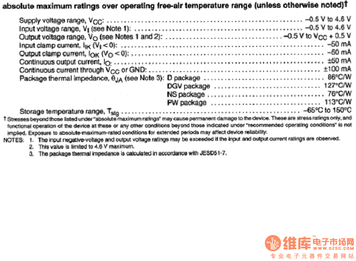 Figure 2. Example of Absolute Maximum Ratings Section ͼ2���������ֵһ�ڵ�ʾ�� * - ���������ʱ�䣺2005-4-24 0:47:48 ���ߣ�IC921 |
|||||||||
| 30¥�� | >>�������� |
| ���ߣ� asunmad �� 2005/4/16 13:44:00 ������
�о�convention����Ϊ��Լ�е㷨�������ζ�� �Ҿ��ýй�������Щ�� [008] All limits are given according to the absolute-magnitude convention, with a few exceptions. �����������⣬����ֵ���ǰ��վ���ֵ���ȹ��������ġ� |
|
| 31¥�� | >>�������� |
| ���ߣ� kasami �� 2005/4/16 14:45:00 ������
conventionҲ�뷭��ɡ��������ģ���������ĸо������� |
|
| 32¥�� | >>�������� |
| ���ߣ� ic921 �� 2005/4/16 18:59:00 ������
��....also known as features bullets�� ���°汾 * - ���������ʱ�䣺2005-4-16 19:19:52 ���ߣ�ic921
|
|

| 33¥�� | >>�������� | ||||||||||||||||||||||||||||||||||||||||||||
| ���ߣ� kasami �� 2005/4/16 19:34:00 ������
TI�������·��룺���������ֲ�������ŵĽ���������(5) Recommended Operating Conditions�Ƽ���������
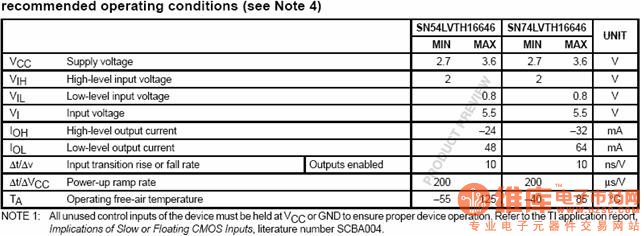 Figure 3. Example Recommended Operating Conditions Section ͼ3���Ƽ���������һ�ڵ�ʾ�� NOTE 1: All unused CONTROL inputs of the DEVICE must be held at VCC or GND to ensure proper DEVICE operation. REFER to the TI application report, Implications of Slow or Floating CMOS Inputs, literature NUMBER SCBA004. * - ���������ʱ�䣺2005-4-24 0:52:12 ���ߣ�IC921 |
|||||||||||||||||||||||||||||||||||||||||||||
| 34¥�� | >>�������� |
| ���ߣ� ic921 �� 2005/4/16 21:14:00 ������
Switching characteristics�Ƿ����������˲̬���ԡ��� to akaer : ��ԭ�ĵ��ң��Ƕȿ�����һ�����ǵ���������ֱ������ģ���ˣ�����Ϊ���ˡ� ������û�в鿴ԭ�ģ�ֻ�뵽��̬�����ȥ�ˡ� _____________________ �Բ����ҿ�����������ȥ�ˣ����ǶԵ�! * - ���������ʱ�䣺2005-4-16 23:23:29 ���ߣ�ic921 |
|
| 35¥�� | >>�������� |
| ���ߣ� kasami �� 2005/4/16 21:46:00 ������
���akaer Switching characteristics �Ƿ����������˲̬���ԡ��� ��������仰ʱ�����Dz��⣬�����뵽����ŷ��֣�ȷʵӦ����ô�� Timing requirements ��Ҳ��������ʱ��Ҫ��������ʱ���Ǹ��� |
|
| 36¥�� | >>�������� |
| ���ߣ� kasami �� 2005/4/16 22:03:00 ������
���������ing |
|
| 37¥�� | >>�������� | ||||||||||||||||||||||||
| ���ߣ� kasami �� 2005/4/16 23:22:00 ������
TI�������·��룺���������ֲ�������ŵĽ��������⣨6�� Electrical Characteristics��������
 Figure 4. Example Electrical-Characteristics Section ͼ4����������һ�ڵ�ʾ�� ԭͼע�ͣ� On products compliant to MIL-PRF-38535, this parameter is not production tested. All typical values are at VCC = 3.3 V, TA = 25��C. Unused pins at VCC or GND This is the bus-hold maximum dynamic current. It is the MINIMUM overdrive current required to SWITCH the input from one state to another. This is the increase in supply current for each input that is at the specified TTL voltage level, rather than VCC or GND. Live-Insertion Specifications��������
Timing Requirementsʱ��Ҫ��
Switching Characteristics˲̬����
Live-insertion specifications for B PORT over recommended operating free-air temperature range  Figure 5. Example Live-Insertion Section ͼ5 ����С��ʾ�� * - ���������ʱ�䣺2005-4-24 0:56:42 ���ߣ�IC921 |
|||||||||||||||||||||||||
| 38¥�� | >>�������� |
| ���ߣ� asunmad �� 2005/4/17 8:32:00 ������
comments: address, etc. [023] This section addresses the timing relationships between transitions of one or more input signals that are necessary to ensure DEVICE functionality and applies ONLY to sequential-logic DEVICEs (e.g., flip-flops, latches, and registers). ����Ϊһ������������ź�֮���ʱ���ϵ�ṩѰַ����Щ�����ź���ʹ�����������õı����źţ�����ֻӦ����˳�������� �����紥����������Ĵ����ͼĴ������� �ⲿ������ֵ���̴_�� ����е�address���ǡ�Ѱַ������˼���ǡ�������������������⡱����˵����ijij���⣩������˼�� ����ṹ�Ͽ���ȫ��Ϊһ�����о䣨�������Ӿ䣩����addresses������applies�������У�����Դ�applies���������� ���룺 ����˵��һ�����������źŵ�ת����֮���ʱ���ϵ����Щʱ���ϵ�Ա�֤�����Ĺ����DZ���ġ�����ֻ������ʱ���·���紥�������������ͼĴ������� ���⣬��[020]�ε�under the conditions in the recommended operating conditions table����Ϊ�����Ƽ����������¡�����˼�Ѿ������ﵽ�ˣ����Ҳ�������ô���롣��Ϊ�����Ƽ����������¡���Ӣ����ȫ����˵�ɡ�under the recommended operating conditions��������˵����Ӣ����Ҳ˿������ԭ���е�˵���ֿڻ���Ƨ��ԭ�IJ����˸��߳���˵����������ΪӢ���뺺��IJ��죬����ȫд�����IJ��죬�������Ӧ�������������ֳ��������ҡ�recommended operating conditions table����һ��ʵʵ���ڴ��ڵı�������Ϳ���֪������ֱ��ȥ���������ԣ��Ҿ���ԭ����Ϊ�����Ƽ����������������涨�������¡��Ƚ���ʵԭ�ġ� |
|
| 39¥�� | >>�������� |
| ���ߣ� kasami �� 2005/4/17 10:26:00 ������
sequential-LOGIC DEVICEs ��ʱ���·���� DEVICE ������ʱ���ǡ� ����,�豸,װ�á�����˼���и����LOGIC DEVICE �ǡ� ���豸������˼��¥�ϵİ�sequential-LOGIC DEVICEs ����� ��ʱ���·������ѧ���е㲻�⣬����ϸָ�̣������� ���⣬[020]�Ǿ仰��������Ǻܺã����̲�ס��Ҫ˵һ�Ρ�������� |
|
| 40¥�� | >>�������� |
| ���ߣ� asunmad �� 2005/4/17 13:02:00 ������
sequential-logic DEVICE: ʱ�������� ��д�ɡ�ʱ���·������Ϊƽʱ˵�����˵ϰ���ˣ���ʱ����������ȷЩ������Ȼ���ǵ���˼��ࡣ sequential������϶�����ɡ�ʱ�ȽϷ����й���½��ϰ�ߣ������롰Combinational������ϵģ����Ӧ�ġ� PS: ���⣬[020]�Ǿ仰��������Ǻܺã����̲�ס��Ҫ˵һ�Ρ�������� �⻰�����е㲻�Ծ���~~~~�ҵ�һ�е����������ڼ��������̽�֣�����֮���������~~~~ * - ���������ʱ�䣺2005-4-17 13:07:42 ���ߣ�asunmad |
|
| 41¥�� | >>�������� |
| ���ߣ� asunmad �� 2005/4/19 7:23:00 ������
features bullets�е�bullet��������Ӧ��bulletin �����ϵ�ȷ�����ҵ�features bulletin��features bulletin board��˵��������ʹ��ˣ���Ҳ�Ҳ������ʵķ��롣 |
|
| 42¥�� | >>�������� | ||||||||||||
| ���ߣ� kasami �� 2005/4/20 22:49:00 ������
���ַ��룺TI���������ֲ�������ŵĽ��������⣨7�� 2.8 Noise Characteristics��������
noise characteristics, VCC = 5 V, CL = 50 pF, TA = 25��C (see Note 4)  NOTE 2: Characteristics are for surface-mount packages ONLY. Figure 8. Example Noise-Characteristics Section ͼ8����������С�ڵ�ʾ�� 2.9 Operating Characteristics��������
operating characteristics, TA = 25��C  Figure 9. Example of Operating-Characteristics Section Parameter Measurement Information ͼ9����������С�ڲ���������Ϣ��ʾ�� 2.10 Parameter Measurement Information����������Ϣ
 Figure 10. Example Parameter Measurement Information Section ͼ10������������ϢС�ڵ�ʾ�� ˵����ԭ��û��С�ڱ�ţ��Ķ���̫���㡣�ӱ��������߶�ԭ�ĵķֽ����˼�עС�ڱ�ŵĴ���������ط����в��ף������λ����ָ���� * - ���������ʱ�䣺2005-4-20 23:14:48 ���ߣ�IC921 |
|||||||||||||
| 43¥�� | >>�������� |
| ���ߣ� ic921 �� 2005/4/24 0:37:00 ������
CMOS POWER Consumption and Cpd Calculation CMOS POWER Consumption and Cpd Calculation ���ӣ�http://focus.ti.com/lit/an/scaa035b/scaa035b.pdf http://focus.ti.com/lit/an/scaa035b/scaa035b.pdf |
|
| 44¥�� | >>�������� |
| ���ߣ� gyfeng1017 �� 2005/4/27 13:23:00 ������
̫���� �������һȦ,����ѧ�����ٶ���.�Ժ���Ҫÿ�춼���������ѧӢ��.�����Ӣ�ķ��붼�ܲ���. |
|
| 45¥�� | >>�������� |
| ���ߣ� kasami �� 2005/5/10 11:58:00 ������
ʵ�ڱ�Ǹ�� 51�ڼ���ϸ����һ����ƪ���£����ñ�ƪ���ҵ�רҵ�����нϴ���룬�ܶ����ʶ�����˵�dz�İ������˵���������ɽ���������룬�о��������ġ�ʱ����ȣ��һ����뽫ʱ�����õ��Լ���רҵѧϰ��ȥ����˼����������ٷ�����ȥ�ˡ��ڴˣ���л��λ��֧�֣����λ������ԭ�¡� ���⣬�ڷ����������ݵĹ����У�һλ���Ѹ����Һܶ����潨�飬�ڴ˱�ʾ��л�� |
|
| 46¥�� | >>�������� |
| ���ߣ� kasami �� 2005/5/10 19:39:00 ������
����λԸ���������Ļ�������ֱ�Ӻ�IC921��ϵ ���ڲ��ܼ�����������飬����ʮ�ֱ�Ǹ���ղŰ���IC921����Ϣ˵�����ҾͰ�Ȩ�������ٽ���һ�£��Ҿ���ʮ�ֲ������ҷ��������Ҳ���ֻ࣬�Ƿ��������һ��ѧϰ���������Ѿ�ֹͣ�����ˣ���Ȩ������ͺ������ˡ������λԸ���������Ļ�������ֱ�Ӻ�IC921��ϵ����������ԭʼ���ϡ���������ллIC921�ˡ� ���⣬�ҵ��û�������ת�������ˣ�������ƪ���뵽���ܷ������ȥ����kasami����û���û�й�ϵ�ˡ� ���лл��λ��֧�֡� |
|
| 47¥�� | >>�������� |
| ���ߣ� IC921 �� 2005/5/11 19:57:00 ������
���Ѿ�����һЩ����һ���Ƚ��� ллkasami���Ȿ���Dz��ܵ����Լ�ѧϰ�����Ŀ���/ҵ�������Ŵ�һ�����ġ�������˽������������꣬��Ȩ�������һ�úÿ�����ġ� ���������־��ף����ɾͣ��� |
|
| 48¥�� | >>�������� | |||||||||||||||||||||||||||||||||||||||||||||||||||||||||||||||||||||||||||||||||||||||||||||||||||||||||||||||||||||||||||||||||||||||||||||||||||||||||||||||||||||||||||||||||||||||||||||||||||||||||||||||||||||||||||||||||||||||||||||||||||||||||||||||||||||||||||||||||||||||||||||||||||||||||||||||||||||||||||||||||||||||||||||||||||||||||||||||||||||||||||||||||||||||||||||||||||||||||||||||||||||||||||||||||||||||||||||||||||||||||||||||||||||||||||||||||||||||||||||||||||||||||||||||||||||||||||||||||||||||||||||||||||||||||||||||||||||||||||||||||||||||||||||||||||||||||||||||
| ���ߣ� IC921 �� 2005/5/11 20:03:00 ������
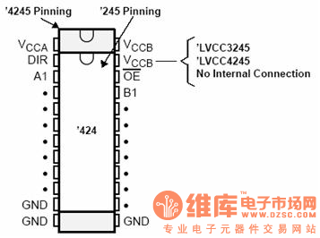
���ַ��룺TI���������ֲ�������ŵĽ���������029��032�� 3.1 Summary DEVICE DESCRIPTION ��������ժҪ3.1.1 Title, Literature NUMBER, and Dates of Origination and Revision���⡢���ױ��롢����Դ�Ͱ汾
Example ʵ��: 
| ||||||||||||||||||||||||||||||||||||||||||||||||||||||||||||||||||||||||||||||||||||||||||||||||||||||||||||||||||||||||||||||||||||||||||||||||||||||||||||||||||||||||||||||||||||||||||||||||||||||||||||||||||||||||||||||||||||||||||||||||||||||||||||||||||||||||||||||||||||||||||||||||||||||||||||||||||||||||||||||||||||||||||||||||||||||||||||||||||||||||||||||||||||||||||||||||||||||||||||||||||||||||||||||||||||||||||||||||||||||||||||||||||||||||||||||||||||||||||||||||||||||||||||||||||||||||||||||||||||||||||||||||||||||||||||||||||||||||||||||||||||||||||||||||||||||||||||||||