|
|||||||||||
| �������� | ��·���� | ������� | ���ֹ�� | ͨ�ż��� | ��Դ���� | ���֮�� | EMC���� | ARM���� | EDA���� | PCB���� | Ƕ��ʽϵͳ ������� | ���ɵ�· | �����滻 | ģ�⼼�� | ������ | �� Ƭ �� | DSP���� | MCU���� | IC ��� | IC ��ҵ | CAN-bus/DeviceNe |
ȫ���������ʧ�洢��(Flash,EPROM,EEPROM) PDF�����ṩ���� |
| ���ߣ�code631����Ŀ�����ɵ�· |
�����ܶ������ʼ�����ʧ�洢�������⣬��ͷ��һ�ݺܺõIJ��ϣ����Ǿ��з�������ĸ�������۵���ͷ��ϣ���ܸ����һЩ������ PDF Version download here: http://file.21ic.com.cn/songfei/17���ۺ�������/ȫ���������ʧ�洢��.pdf ��Ȩ������ ������Ϊ������Ʒ ԭ���ߣ�Jitu J.Makwana, Dr.Dieter K.Schroder �����ߣ�GongYi��INFINEON TECHNOLOGIES, MEMORY development center�� email: code631@gmail.com ת����ע��������Ϣ��лл������ * - ���������ʱ�䣺2006-3-30 15:48:06 ���ߣ�code631 |
| 2¥�� | >>�������� |
| ���ߣ� code631 �� 2005/12/21 0:28:00 ������
����ʧ�洢������ ����ʧ�洢������ ���ߣ�Jitu J.Makwana, Dr.Dieter K.Schroder ���룺GongYi(INFINEON TECHNOLOGIES,MEMORY development center�� Email: code631@gmail.com ǰ�� ���������˻�������ʧ�洢����NVM���Ļ��������һ���ֽ�����NVM�Ļ������������NVM�ı����Լ����õĴ洢������ڶ������ҽ���������ͨ���ȵ���ע��ʵ��NVM�ı�̡��������ְ�������FOWLER-NORDHEIM ����ЧӦʵ�ֶ�NVM�IJ�����ͬʱ����FN����ЧӦ��ԭ��Ҳ��������������һ��˵�������IJ��ֽ���������Ԥ��NVM������Ե�ģ�͡��ȵ���ע������������ġ����˵��ӡ�ģ�͡����һ���ֽ�����NVM�ɿ��Է�������⣬�����ݱ���������DATA RETENTION��,�;�����ENDURANCE��,���ţ�DISTURB���� �ؼ��֣�����ʧ���洢�����ȵ���ע�룬����ЧӦ���ɿ��ԣ����ݱ��֣��;��������ţ����� * - ���������ʱ�䣺2006-4-1 7:13:14 ���ߣ�code631 |
|
| 3¥�� | >>�������� |
| ���ߣ� code631 �� 2005/12/21 0:29:00 ������
��һ���֣� ���� ��һ���֣� ���� �洢�����¿ɷ�Ϊ�����ࣺ��ʧ�ͷ���ʧ����ʧ�洢����ϵͳ�ر�ʱ����ʧȥ�洢���ڵ���Ϣ������Ҫ�����ĵ�Դ��Ӧ��ά�����ݡ��ֵ�����洢����RAM�������ڴ��ࡣ����ʧ�洢����ϵͳ�رջ���Դ��Ӧʱ���ܱ���������Ϣ��һ������ʧ�洢����NVM������ͨ��Ҳ��һ��MOS�ܣ�ӵ��һ��Դ����һ��©����һ���ż������һ����դ��FLOATING GATE�������Ĺ����һ���MOS�����в�ͬ������һ����դ����դ����Ե��������������֡� ����ʧ�洢���ֿɷ�Ϊ���ࣺ��դ�ͺ͵�����͡�Kahng �� Sze ��1967�귢���˵�һ����դ������������������У�����ͨ��3nm��ȵ������������ЧӦ�Ӹ�դ�б�ת�Ƶ�substrate�С�����ЧӦͬʱ�����ڶ��ڼ�ı�̺Ͳ�����ͨ������������������С��12nm�� �����ڸ�դ�еĵ����������Ӱ����������ֵ��ѹ��Vth��,�ɴ������ڼ�״̬����ֵ1��0�� �ڸ�դ�ʹ洢���У���ɱ������ڸ�դ�У���������Դ��Ӧ���������Ȼ���Ա��֡����еĸ�դ�ʹ洢�����������Ƶ�ԭʼ��Ԫ�ܹ������Ƕ��в�����ż��ṹ��ͼһ��ʾ����һ���ż��������ż�������ͼ���������֮�䣬����������������Ǹ�����դ����������ɿ�������-��-�������߶������衣��Χ��������Χ�Ķ����������Ա���������������Ӱ�졣�ڶ����ż�����Ϊ�����ż��������ⲿ�ĵ缫�����ӡ���դ������ͨ������EPROM(Electrically Programmable Read ONLY MEMORY)��EEPROM(Electrically Erasable and Programmable Read ONLY MEMORY)��
|
|

| 4¥�� | >>�������� |
| ���ߣ� code631 �� 2005/12/21 0:31:00 ������
1 ���������������1967�걻�����ģ�Ҳ�ǵ�һ���������ĵ��̰뵼���������������͵Ĵ洢���У���ɱ������ڷ���ĵ����У��ɴ�����Դ��Ӧʱ������Ϣ������������ĵ���Ӧ������MNOS(METAL Nitride Oxide SILICON)��SNOS(SILICON Nitride Oxide SEMICONDUCTOR)��SONOS(SILICON Oxide Nitride Oxide SEMICONDUCTOR)�С�ͼ��չʾ��һ�����͵�MNOS������ʹ洢���Ľṹ��  MNOS�еĵ��ͨ�����ӻ��ƴ���һ�㼫���������㣨һ��Ϊ1.5-3nm���ӹ����б�ע�뵪���С� �����ϵ�һ��EPROM,��һ����դ����������ͨ��ʹ�ø߶Ȳ��ӵĶྦྷ�裨poly-Si����Ϊ��դ���϶��Ƴɵģ�������Ϊ��դѩ��ע����MOS�洢����FAMOS���������ż���������Ϊ100nm, �ɴ˱����������substrate�� �Դ洢���ı����ͨ����©��ƫѹ��ѩ������ʹ�õ�����ѩ���д�©������ע�뵽��դ�С����ִ洢���IJ���ֻ��ͨ�������������X�����䡣�������EPROM�ķ�װ��ʽͨ�����մɴ���һ�������С���ڣ�������һ�����Ϸ�װ��û��ʯӢ���ġ���Щ�洢������Ϊһ���Ա�̴洢����OTP��,���ִ洢���ܱ��ˣ������ڷ�װ��Ҫ���������Dz����ܵġ�����ʯӢ���ڵ�EPROM�۸�ȽϹ������ڿɱ����������Կ����ڷ�װ��������IJ��ԡ� ��Ȼ��70�����������ɲ����͵���ҵ�÷���ʧ�洢�������Ƶ�ɲ�д�ͷ���ʧ�洢�������������������� H.IIZUKA et.al �����˵�һ����ɲ�д�ͷ���ʧ�洢��������Ϊ����ѩ��ע����MOS(SAMOS)�洢����SAMOS�洢���������ྦྷ���ź�һ���ⲿ��������ɡ��ⲿ�����ŵij���ʹ�õ�ɲ�д��Ϊ����ʵ����������˲�����Ч�ʡ���ɲ�д�ͷ���ʧ�洢���ĵ������ͨ������դ�еĵ�����ָ���δע��ʱ��ˮƽʵ�ֵġ������������������Ʒ�����ֲ�Ʒ�ķ�װ�ɱ������ܶࡣȱ���ǵ�λ�洢��Ԫ�ijߴ�Ҫ����ǰ��ܶ࣬ʹ�þ�Ԫ���Ҳ���˺ܶࡣEEPROM��Ԫ�������������ɣ�һ���Ǹ�դ����ܣ���һ����ѡ����ܣ���ͼ����ʾ��ѡ������������ڱ�̺Ͳ���ʱѡ����Ӧ�ĸ�դ����ܡ����������ڼ����˴�λ������·�Լ�����·����Ԫ�ߴ类�ٴ�����  ��80�����һ������ķ���ʧ�洢����Ʒ�������ˣ��Ǿ������档��һ�������Ʒͨ���ȵ���ע�����ʵ�ֶ�������̣������������������ЧӦ���������͵Ĵ洢��ֻ�ܱ���Ƭ��һ�������ɾ�������ܱ����ֽ�ɾ������ˣ�ѡ����ܱ��Ƴ��ˣ��ɴ�Ҳ��С�˵�Ԫ�ijߴ硣���͵ĵ�Ԫ�ṹ��ͼһ��ʾ�� * - ���������ʱ�䣺2005-12-21 0:36:02 ���ߣ�code631 |
|
| 5¥�� | >>�������� |
| ���ߣ� code631 �� 2005/12/21 18:06:00 ������
2 �ڶ����� ������̻��� �����Ǹ�դ�ͻ������ʹ洢������������̶���ͨ��������ע�븡դ�����ߵ������С�ʵ�ִ˹��̣���Ҫ��ͨ�����ֵĻ��ƣ�FN ����ЧӦ���Ա������㣩�Լ��ȵ���ע�롣 1�� Fowler-Nordheim ����ЧӦ FN����ЧӦ��NVM����Ҫ�ĵ��ע�뷽ʽ֮һ���ڶ��������ʱ���ڿ����ż����Ϻܴ�ĵ�ѹ��Vcg�����ܴ��ṹ����ͼ�ı仯��  ��ͼ���У�ec �� ev �ֱ��ǵ����ͽ�����Eg Ϊ�ܴ����� (�������1.1 eV ), fb ΪSi-SiO2 �������� (fb is 3.2 eV for electrons and 4.7 eV for holes). ��ӵ�ѹ Vcg ��ɵ����ṩ��substrate�еĵ���ͨ�����������е��������︡դ���Ŀ��ܡ�������IPD�����������ܴ��Dz�ͬ�ģ������������ǵĺ�Ȳ�ͬ��IPD��ȴ�25nm��45nm���ȣ�������������ֻ��5nm��12nm�����ӵ��︡դ�����γɵĵ����ܶ�Ϊ��    ����, h = ���ʿ˳��� = ��������������� (3.2 eV for Si-SiO2) q = �������ӵ��� (1.6x10⁻¹⁹ C) m = ���ɵ������� (9.1x10⁻³¹ kg) m* = ���������ܴ������ɵ�����Ч���� (0.42 m) Vinj = ע�������� Vapp = ��������������� (V) Vfb = ƽ������(V) tox = ���������� (cm) ��ʽ 1 ���������ܶȺͼ������������������Vapp��ָ���ȣ� �Ӷ�Ӱ������������Vinj��ͼ��չʾ��һ��NVM�ĺ���棬���������ЧӦ�����ɾ��ȷֲ���Vcg ����ѹ��Դ��Vs ��©�� Vd, �Լ�substrate Vsub ���ӵء�  ��һ����ѡ�Ķ�FLASH��̵ķ�����ͼ����ʾ������Ϊ©������ЧӦ���˷�����ʱ�Ⱦ�������ЧӦ����ڱ���ٶȷ��������������ע�������С�����������������ܶȸ���  * - ���������ʱ�䣺2005-12-21 18:07:49 ���ߣ�code631 |
|
| 6¥�� | >>�������� |
| ���ߣ� code631 �� 2005/12/22 20:46:00 ������
������̻��ƣ��ȵ���ע�� 2���ȵ���ע�� NVM Ҳ����ͨ���ȵ���ע����ʵ�ֱ�̡�������p��substrate�ϵ�n��NVMʹ���ȵ���ע�룬����n��substrate�ϵ�p��NVM������ȿ�Ѩע�롣�ȿ�Ѩע����ٶȷdz�����������Ϊ��Ѩ������Si-SiO2 �ܴ����ݣ�4.7 eV ��, ��Ҳ�����ھ������NVM�����̶�����p��substrate��n��NVM��ԭ�� ͨ���洢����Ԫ����©����ж�����դ�������ȵ���ע�롣��Щ�ȵ���ͨ����©��ƫ�õ�ѹ�õ����������ұ�ˮƽƫ�õ�ѹ����Elat������©������ӵ�и��ߵĵ��Ƶĺľ�������Щ���ӵõ��㹻�������Գ���substrate����������֮�����������3.2 eVʱ�����ڼ����������������Vd �������ܹ���ע�����������У���һ���ߵ�������� Vcg �������ڿ����ż�ʱ����Щ���ӱ��������˸�դ���С���ʱ�ܴ��仯��ͼ�ߡ�  ͼ�ߣ���դ�ʹ洢����Ԫ���ȵ���ע��ʱ�ܴ�ͼ ����դ���㹻��������ע���ע�����Ig ������������Ϊ0��������Ϊ���������Eox (�ڿ�ʼʱ������������) �������ų���ӡ�Vcg �����˸�դ�еĵ����ͬʱ Vd ��Ӱ���˱���ٶ�. ͼ��չʾ��һ�������ȵ���ע��ʵ�ֱ�̵�NVM�ĺ���档 Vcg �� Vd Ϊ�����ѹ�ֱ�Ϊ15 V �� 10 V �� Vs �� Vsub ��ӵء�  |
|
| 7¥�� | >>�������� |
| ���ߣ� code631 �� 2005/12/22 20:50:00 ������
�������֣� ������������ �������֣� ������������ �ڶ��������������ֱ�̻��ƣ�FN ����ЧӦ�Լ��ȵ���ע�롣Ϊ���ܹ��ٴζ�NVM��̣�֮ǰ��Ҫ��NVM���������½������ڹ�ҵ���Ӧ�õ�NVM�������ơ� ��ע�븡դ֮�еĵ��ӱ���/�������������ݣ�3.2 eV�����������С�����������/��Ӵ���ĵ�ѹ��������Ҳ����3.0 eV����ˣ� ������ȻǨ�ƵĿ����Ժ�С����դ�ڴ���ĵ���ʹ����������ֵ��ѹ���� ͨ���������ֲ��������� 1. ���������� 2. FN ����ЧӦ IIIa. ���������� ����ͼ����ʾ���������������������㹻�����������Կ˷����������ɸ�դ�����������������substrate���������ڼ����ֵ��ѹ���͡�һ����˵����ֵ��ѹ�Ӹߵ�λ���͵��е�λ����Ҫ��ʱ���ԼΪ10���ӡ�  ͼ�ţ��������NVM���ܴ�ͼ IIIb. FN ����ЧӦ FU ����ЧӦҲ���ڶ�NVM�IJ���������֮һ�ǶԿ����ż��Ӹ߸���ѹ����ʱ�ܴ��仯��ͼʮ��ʾ�����ӵĵ�ѹVcg �γɵĵ糡�����һ���������ݣ�������դ�еĵ����ṩ��һ���ɸ�դ����substrate��ͨ·��  ͼʮ����դNVM����FN����ʱ���ܴ�ͼ ͼʮһa��bչʾ�����ֲ�ͬ��FN������������������ЧӦ��©����������ЧӦ����һ�ַ����У�ֻ��Ҫһ���ܴ�ĸ���ѹ�������ڿ����ż������ڶ��ַ����У����˴˸���ѹ֮�⣬����Ҫ��©������һ������ѹ��   �ܵ���˵����������ЧӦ����Ҫ��©����������ЧӦ�����������Ǻ��߿��ܻ���������ɿ������⣺���ڼ��е���������ɵ�©�������������ƻ��� |
|
| 8¥�� | >>�������� |
| ���ߣ� code631 �� 2005/12/22 20:54:00 ������
���IJ��֣� ��������ע��ģ�� ���IJ��֣� ��������ע��ģ�� �ȵ���ע���Ƕ�FLASH EEPROM��̵�һ���ֶΣ������øߵ糡���ٵõ����ȵ���ע�븡դ����ʵ�ֵ��ӵ��ƶ����˷�������ٶȱȽ�����������Ϊ����ע��Ч�ʺܵͣ��������ǽ����ڿ����Ե�ͳ��ѧ����֮�ϡ��ȵ���ע�����Ҳ������©������ĵ��룬���Ӻ����Ӷ�������������߶��ܵĿ�Ѩͨ����substate���ռ��Ӷ��γ�substrate���� (Isub)��������©�������ռ��γ�©������ (Ids)����ʱ�����������糡(Eox)�������ӣ���ô��Щ�����ӽ��˷���������ͨ�������㵽�︡դ���γ��ż�ע�����(Ig)��������ģ�����������ȵ���ע�룺 1�� ���˵���ģ�� 2�� ��Ч�����¶�ģ�� IVa.���˵���ģ�ͺ���ֵ��ѹ VT ���˵���ģ������Ф�ػ������ģ���������˵��������ô�����ͣ�Ϊ��ʹ�ȵ����ܹ����︡դ�����ȵ��ӱ����ڴ�ֱ�������Ʋ��еõ��㹻�Ķ��� (Elat) ʹ���������㹻�Ķ����˷����������������ݵ���Si-SiO2 �Ӵ���ͼʮ��չʾ�����˵���ģ�͵ĸ��������߱����������� A - B��һ������������Elat �õ�����������ȵ��ӡ����Ķ��ܱ��뱻����������Si-SiO2 �Ӵ��档����˹��̵Ŀ�����Ϊ -- һ�����ӻ�����Կ˷�Si-SiO2�������ݵ������Ŀ����ԡ� B �C C�����ȵ��ӱ��벻�ܱ���ײ��ɥʧ��������һ���̵Ŀ�����ΪPSEMI ��PSEMI ������Ϊһ��������Si-SiO2 �Ӵ��洩����������ײ�Ŀ����ԡ� C �C D�� ������Si-SiO2 �Ӵ����ƶ�����դ�������У������벻���������еĵ��������������˹��̵Ŀ�����ΪPinsul �C ���Ӳ����������е������������Ŀ����ԡ�  ͼʮ�������˵���ģ���ܴ�ͼ ��������������������ͳ��ѧ�ϻ���������ܿ����Լ�Ϊ����֮�˻�����ô�ż��������Եó���  ���У� lr = ����ɢ��ƽ��·������ = 92 nm Leff = ��Ч�������� (cm) Ids = ©��- Դ������(A) ��դ���ĵ�����ı�����������ֵ��ѹ��  ���У� DVT = VT (Programmed) - VT (Initial) DQfg = Qfg (Programmed) - Qfg (Initial) = ��դ��������仯 ������仯Ҳ����  ���У�DtΪ���ʱ�䣨s�� ������ֵ��ѹ�ɳ�ʼֵ�����ڵı仯Ϊ��  ���У� Cfg = ��դ�������ż��ĵ�����(F) ͼʮ��չʾ��һ�����͵Ĵ����������ߣ����Կ���Ids-Vcg �������ƽ�еġ����ǵ�λ���൱��DQfg/ Cfg��  |
|
| 9¥�� | >>�������� |
| ���ߣ� code631 �� 2005/12/22 20:59:00 ������
���岿�֣� NVM�ɿ������� ���岿�֣� NVM�ɿ������� NVM�洢����Ԫ�м�����Ҫ�Ĺ����Բ���������������Ԫ�����ܡ���Щ�����������Է�Ϊ�����ࣺ�;��������ݱ���������Ϊ�˸��õ�������Щ��������б�Ҫ�˽�һЩ�����������㣬IPD��������֪ʶ��������EPROM�� EEPROM����FLASH EEPROM�У�Ӱ�������ɿ��ԵĹؼ��������������IPD�������� ����������Ҫ��ʧЧ�����漰�����ȵ��ӻ���FNע��ʱ�ɸߵ糡�������������������ݡ����о�����������ȱ�ݺ����ݶ���������ݡ����������ͨ��������ͨ����λ����ĵ������(Qbd)����һ��ˮƽ֮��ͨ��Ҳ����ӵ糡ǿ���йء�Qbd�Ǹ���ҵ���������ܲ��ԣ����ڲ����������ڸ�Ũ��Qbd����µı��֡����ݵĶ������ڶԵ�Ԫ���ʱ��ɵĵ������������б���ס��������������ı���ע�������������ԣ���ˣ���ת�Ƶ���դ���ĵ��������Լ������ֵ��ѹҲ���ı䡣 ��ǰ�Ѿ��ᵽ��IPD,��ͨ�����ڸ�����դ��������������������������������ȱ���Է�ֹ©�����IJ��������ڸ�դ���ɶྦྷ�蹹�ɵģ�ͨ������IPD�������չ����б������ġ������Ĺ��̵�����grain ��Ե��ǿ�Ӷ��ı��˶ྦྷ�����������ṹ���γ���С¡��״���档��Щ����IJ�ƽ�������˾ֲ��糡�ı仯�������˸�©������Ӱ��IPD����������һ�������Ƕྦྷ���IJ��ӺͶྦྷ�����������ʱ���¶ȿ��ơ����־�Ե���ϲ��ã����Լ���ȱ���ܶȺ���ߵ糡���ȶ�����-��-�����ڱ��㷺Ӧ����IPD���Է�ֹ©�����IJ������ڴ˲����У���դ���ӱ���������ס���Ӷ��γ���©��������ĵ糡����һ����С©����������ͨ��ONO����Ϊ5 - 10 nm���ײ�������, 20 nm�����㣩, 3 nm���������������ײ��������ڸ�դ�����棬����������λ�ڿ����ż����档  ͼʮ�ģ����ڱ��治ƽ��������IPD ©���� Va. �;������� �;������Ա����ڴ洢������ֵ��ѹ���䣬�����̴��������еĹ�ϵ����ͼʮ����ʾ��NVM���Ա���̺Ͳ���ֱ�������㱻�ƻ�����Ҳ��ζ��NVM��Ч�Ŀɱ�̴��������ģ�������˵������EEPROM��Ʒ���Ա�֤106 ��Ч��̴��������������������ƻ�ͨ������Ϊ������Ľ�������һ���洢�����Ծ��ܵ�����̴�������Ϊ�;�������ֵ��ѹ���ڹر�ͨ������������ֵ���ߵ�ƽ��͵�ƽ״̬��̫С�������ܱ��������֡������������ڵ��ӱ���������ԭ�еĵ�����������ס�����ƶ�������ʵ��֤���������ڶԵ�Ԫ��̻��߲������������������˼��صĸߵ糡�������ġ���ˣ�����������������������;���������Ҫ��  ͼʮ�壬���͵�EEPROM��Ԫ��ֵ��ѹ���ڹر� Vb. ���ݱ����������� ��һ��NVM��Ԫ�����ָ�դ�еĵ����ʱ�����dz�֮Ϊ���ݱ���������ɥʧ�����ݱ��������Ǻ���һ��NVM�洢����Ԫ����Դ��Ӧ����¿��Ա������ݵ�ʱ�䡣�ڸ�դ�ʹ洢���У��洢�ڸ�դ���ĵ�ɻ�ͨ�����������IPD��ʧ�������ɵ��ӣ����ӣ��ƶ�����������ȱ����������©�������ᵼ�µ�Ԫ��ֵ��ѹ�ĸı䡣��ͬ�ĵ�����ʧ��ʽ�У��¶�����ĵ��룬�����кͣ�������������Ⱦ��������ʧ��Ϊ����ߵ�Ԫ�ı����������������Dz����˲�ͬ���ֶ���������������IPD�������� ���ݱ������������ù��������������������������ʧ����ʱ����Ԫ����ֵ��ѹ�仯���£�  ����dQFG, CFG, �� dVT �ֱ�Ϊ��դ����ɱ仯����դ�������͵�Ԫ��ֵ��ѹ����ʽ9չʾ����ʧ���ӵ���������ʽ10��չʾ����ʧ�����������γɵ�©�����Ĺ�ϵ�Լ�����ʱ�䡣   ���ڵ��͵� CFG = 30 fF �� VT �仯Ϊ3 V���Ӹ�դ������������������ʧ������ ��ԼΪ 5.6x10⁵�������� 1 չʾ�˱���ʱ�� dt�����ڲ�ͬ�� ILeakage �����5.6x10⁵ ������ʧ���൱��3 V VT�仯�� Leakage Current, ILeakage (A) Retention Time, dt (Years) 1x10-20 0.28 5x10-21 0.56 1x10-21 2.84 5x10-22 5.68 2.85x10⁻²² 10 ����һ�����ݱ���ʱ����ILeakage �ɱ�һ���Կ�����ͨ��NVM��ֵ��ѹ����3V��©����Ϊ2.85x10⁻²² A��������ܹ���Ҫ10�ꡣ Vc�洢������ ���ģ����������ʹ��NVM��Ҫ���Ǿ���10�����ϵ����ݱ���������һ���洢����Ԫ�����ڱ�̺Ͳ����о���STRESS����Ϊ���š�������������֣�dc erase, dc program, program disturb,��read disturb���ڱ�̹�������������ָ�����dc program��program disturb���ڲ������������������dc erase������ڶ������еĸ��ű���Ϊread disturb��ͼʮ��չʾ��һ���洢����Ԫ���е�·ͼ�����������ڽ���������  ͼʮ�������ڽ���������ĵ�·ͼ ����ͼ�У��洢����Ԫ���е���������ÿ����Ԫ��©����(COL 1, COL 2, and COL 3) ����Ϊλ�ߣ������е���������ÿ����Ԫ�Ŀ����ż� (ROW 0 and ROW 1) ����Ϊ���ߡ���ǰ������ȵ���ע����������Ѿ�˵�����ڶԴ洢�����ʱ��Ҫͬʱ��λ�ߺ������ص�ѹ�� ���������������ֲ�ͬ�ĸ��ţ� 1) DC Erase: �������͵ĸ���ͨ���������Ѿ�����̵ĵ�Ԫ(Cell A)����Щ���뱻��̵ĵ�Ԫ��ͬһ������ (ROW 1) �ĵ�Ԫ���ڱ����(COL 2 and ROW 1)���ڴ��ڼ�ROW 1 ������һ���ߵ�ѹ15 V���ɴ˲�����һ���ߵ糡������IPD�����ࡣ�����ѹ���ܵ��µ��ӴӸ�դ���ƶ�����������������ǵ����ʧ��ɵ�Ԫ����ֵ��ѹ��С�� 2) DC Program: Ҳ����Ϊgate disturb�������ڵ�δ����̵Ļ����Ѳ����ĵ�Ԫ (Cell B)����Щδ��̵ĵ�Ԫ�����ڱ���̵ĵ�Ԫ��ͬһ������ (ROW 1) ����Щ��Ԫֻ�к������ĵ����ڸ�դ�У�������ǵ���ֵ��ѹ�ǵ͵�ƽ�ġ���ROW1����15Vʱ��ͨ���ż�������ĵ糡��ñ��ú�ǿ����һ�糡���ܵ��µ��ӽ��븡դ���Ӷ������ֵ��ѹ����������£����dz�֮Ϊ����̡� 3) Program Disturb: ͨ��Ҳ��Ϊdrain-disturb��ֻ�����ڱ���̹��ĵ�Ԫ��һ������̹��ĵ�Ԫ (Cell C) �����ڱ���̵ĵ�Ԫ (COL 2 �� ROW 1)����һ��λ�ߡ������ĸ�դ/©������һ���ߵ糡���ڡ���һ�ߵ糡�����˵��ӴӸ�դ������©�����Ӷ�������ֵ��ѹ��С�� 4) Read Disturb: ���ָ��Ż��Ʒ����������ڱ����ĵ�Ԫ����һ�����ߵIJ������ĵ�Ԫ�������������ϵIJ�����ѹΪ5V����ѡ�еĵ�Ԫ©��ƫ��Ϊ1V��δѡ��Ԫ��Դ����©������substrate��Ϊ0V�� |
|
| 10¥�� | >>�������� |
| ���ߣ� code631 �� 2005/12/22 21:00:00 ������
VI. ���� VI. ���� ������Ҫ������NVM�ķ�չ���̺ͼ����ſ�����Ҫ�ı���ֶ�����������ע���FN����ЧӦ����FN����ЧӦ�У��ż���������һ��С��12nm�������ȵ���ע���п��Ժ�ܶࡣ���ֵ��͵IJ�������Ϊ���������FN����ЧӦ��ͨ����UV EPROM��ʹ��������������ķ���������EEPROM��FLASH�洢������ʹ����FN����ЧӦ�������ơ�������������ʱ��һ��Ϊ10���Ӷ�FN����ЧӦ������ʱ����ݿ����ż���©���ϼ��صĵ�ѹǿ�Ȳ�ͬ��Ϊ1ms��10ms�����ı�̻������ȵ���ע�룬һ��ֻ��100MS���ڴ˹����У��������������˵���ģ�ͣ����ģ�ͽ�ʾ���ŵ��������ͨ��������ģ��������Ĺ��̡���Ȼע���Ч�ʺܵͣ������ȵ���ע�븡դ�Ĺ����Ǻܿ�ģ�������Ϊ�����ǿ�糡�����á�����ÿ��NVM������˵���ɿ��Ե����ⶼ���ڣ����;��������ݱ�����������Ҫ���������⡣���⣬�ڱ���кͲ����в����ĸ���Ҳ��Ӱ��NVM�ɿ��Ե�һ�����ء� References [1] Kahng, D. and Sze, S. M. (1967) A floating gate and its application to MEMORY DEVICEs. Bell Systems Technical Journal. 46, 1283. [2] Wegener, H. A. R, Lincoln, A. J., Pao, H. C., O'Connell, M. R., and Oleksiak, R. E. (1967) The variable threshold TRANSISTOR, a new electrically alterable, non-destructive read-only storage DEVICE. IEEE IEDM Technical Digest. 1. [3] Wegener, H. A. R, Lincoln, A. J., Pao, H. C., O'Connell, M. R., and Oleksiak, R. E. (1967) Metal-insulator-SEMICONDUCTOR TRANSISTOR as a non-volatile storage element. International Electron Devices Meeting. (Abstracts). 58 [4] Frohman-Bentchkowsky, D. (1970) The metal-nitride-oxide-SILICON (MNOS) TRANSISTOR-characteristics and applications. Proceedings of IEEE. 58, 1207. [5] Yatsuda, Y., Hagiwara, T., Kondo, R., Minami, S., and Itoh, Y. (1979) N-channel Si-gate MNOS DEVICE for high speed EAROM. Proceedings 10th Conference in Solid State Devices. 11. [6] Suzuki, E., Hiraishi, H., Ishi, K., and Hayashi, Y. (1983) A low voltage alterable EEPROM with metal-oxide-nitride-oxide-SEMICONDUCTOR (MONOS) structure. IEEE Transactions on Electron Devices. ED-30, 122. [7] Frohman-Bentchkowsky, D. (1974) FAMOS-A new SEMICONDUCTOR charge storage DEVICE. Solid State ELECTRONICS. 17, 517. [8] Iizuka, H., Masuoka, F., Sato, T., and Ishikawa, M. (1976) ELECTRICally alterable avalanche-injection type MOS read-only MEMORY with stacked-gate structures. IEEE Transactions on Electron Devices. ED-23, 379. [9] Masuoka, F., Asano, M., Iwahashi, H., and Komuro, T. (1984) A new FLASH EEPROM cell using triple poly-Si TECHNOLOGY. IEEE IEDM Technical Digest. 464. [10] Yeargain, J. and Kuo, K. (1981) A high density floating gate EEPROM cell. IEEE IEDM Technical Digest. 24. [11] Guterman, D., Rimawi, I., Chiu, T., Halvorson, R., and McElroy, D. (1979) An electrically alterable nonvolatile MEMORY cell using a floating gate structure. IEEE Transactions on Electron Devices. ED-26, 576. [12] Lezlinger, M. and Snow, E. H. (1969) Fowler-Nordheim tunneling in THERMALly grown SiO2. Journal of Applied PHYSICS. 40, 278. [13] Tam, S., Ko, P., and Hu, C. (1984) Lucky-electron MODEL of channel hot-electron injection in MOSFET's. IEEE Transactions on Electron Devices. ED-31, 1116. [14] Takeda, E., Kume, H., Toyabe, T., and Asai, S. (1982) Submicrometer MOSFET structure for minimizing hot-carrier generation. IEEE Transactions on Electron Devices. ED-29, 611. [15] Shockley, W. (1961) Problems related to p-n junctions in SILICON. Solid-State ELECTRONICS. 2, 35. [16] Harari, E. (1978) Dielectric breakdown in electrically stressed thin films of THERMAL SiO2. Journal of Applied PHYSICS. 49, 2478. [17] Modelli, A. and Ricco, B. (1984) ELECTRIC field and current dependence of SiO2 intrinsic breakdown. IEEE IEDM Technical Digest. 148. [18] DiMaria, D. J. and Kerr, D. R. (1975) Interface effects and high conductivity in oxides grown from polycrystalline SILICON. Applied PHYSICS Letters. 27, 505. [19] Faraone, L. (1986) THERMAL SiO2 films on n+ polycrystalline SILICON: ELECTRICal conduction and breakdown. IEEE Transactions on Electron Devices. ED-33, 1785. [20] Mori, S., Kaneko, Y., Arai, N., Ohshima, Y., Araki, H., Narita, K., Sakagami, E., and Yoshikawa, K. (1990) Reliability study of thin inter-poly dielectrics for nonvolatile MEMORY application. Proceedings 1985 IEEE IRPS. 132. [21] Aminzadeh, M. (1988) Conduction and charge trapping in polySILICON nitride-oxide-SILICON structures under positive gate bias. IEEE Transactions on Electron Devices. ED-35, 205. [22] Shiner, R. E. (1980) Data retention in EPROMs. Proceedings IRPS. 238. [23] Mielke, N. (1983) New EPROM data-loss mechanisms. Proceedings IRPS. 106. [24] Verma, G. and Mielke, N. (1988) Reliability aspects of ETOX based FLASH memories. IRPS Proceedings, 158 |
|
| 11¥�� | >>�������� |
| ���ߣ� HIGHWAY �� 2005/12/24 21:34:00 ������
����,������ |
|
| 12¥�� | >>�������� |
| ���ߣ� sjb21ic �� 2005/12/25 14:09:00 ������
�����и���Ĺ���MEMORY�Ľ��� лл |
|
| 13¥�� | >>�������� |
| ���ߣ� ljq0746 �� 2005/12/27 23:09:00 ������
��������Զ��δ�ÿһ���û��ĵ绰����ĵ绰�� ������ũ���յ绰�Ѷ���ÿ���µ��յ绰�ѵ�ʱ��һ��һ�Ҵ�绰ȥ��֪����Ҫ�����绰���أ��������Ƚ��鷳��������Ҫ�ܶ��ʱ�䣬Ҳ�Ƚ��飬�õ���ȥ���ɱ���̫���أ�����ũ�������Ա���ò��������������һ�ֵ�·�����Զ��δ�ÿһ���û��ĵ绰���룬���е�������ʾ�ͺ��أ� �����λ���æ������һЩָ��������ũ���յ绰�ѵġ���������Щ������·�� �ҵ�QQ�ǣ�258118704 |
|
| 14¥�� | >>�������� |
| ���ߣ� xinglanp �� 2006/1/17 20:25:00 ������
лл�ˣ������ˣ� |
|
| 15¥�� | >>�������� |
| ���ߣ� enddy �� 2006/1/19 9:15:00 ������
���ºܲ������� ������ĺܲ�������л¥����˳����һ�£���û��NAND�ͺ�NOR��FLASH�ľ������ϣ��������˽�һ�£� |
|
| 16¥�� | >>�������� |
| ���ߣ� tomhe666 �� 2006/1/21 0:21:00 ������
Ϊʲôż������ |
|
| 17¥�� | >>�������� |
| ���ߣ� iC921 �� 2006/1/31 0:37:00 ������
�úúÿ��� |
|
| 18¥�� | >>�������� |
| ���ߣ� iC921 �� 2006/1/31 0:40:00 ������
ԭ������������������ |
|
| 19¥�� | >>�������� |
| ���ߣ� iC921 �� 2006/1/31 0:53:00 ������
�е㡰�鷳�����൱���������� ȫ���������ʧ�洢��(FLASH,EPROM,EEPROM) --ҳ����� -------------------------------------------------------------------------------- [���ڣ�2006-1-3 15:59:08]��������������Դ��21ICBBS���������������ߣ�code631������������: 0 �����ܶ������ʼ�����ʧ�洢�������⣬��ͷ��һ�ݺܺõIJ��ϣ����Ǿ��з�������ĸ�������۵���ͷ��ϣ���ܸ����һЩ������ ��Ȩ������ ������Ϊ������Ʒ ԭ���ߣ�Jitu J.Makwana, Dr.Dieter K.Schroder �����ߣ�GongYi��INFINEON TECHNOLOGIES, MEMORY development center�� email: code631@gmail.com ת����ע��������Ϣ��лл������ ------------------------------------------------- http://www.18ic.com/Html/memory/2006010331.html �����ǣ۱�վ����: �ƹ���ղ����������ղ���������Ʒ����ݵ� http://www.18ic.com/html/memory/2006010331.html |
|
| 20¥�� | >>�������� |
| ���ߣ� iC921 �� 2006/1/31 1:00:00 ������
����ԭ�� A Nonvolatile MEMORY OverviewBy Jitu J. Makwana, Dr. Dieter K. Schroder*A Nonvolatile MEMORY Overview Jitu J. Makwana, Dr. Dieter K. Schroder* E-mail: j.makwana@worldnet.att.net, *schroder@asu.edu This paper presents a basic nonvolatile MEMORY (NVM) overview. Section I begins with the introduction including a brief background of NVM's and the common terms used in the MEMORY industry. The DESCRIPTION and explanation of how an NVM is programmed (adding electrons) using hot-carrier injection is covered in section II. Section III covers the erasing or removing of electrons from floating gates of NVM's. A brief mechanism of Fowler-Nordheim tunneling is covered. Section IV introduces the MODEL that can be used to predict the NVM PROGRAMMING characteristics. The hot-carrier injection MODEL addressed is the "Lucky Electron" MODEL. Section V covers the reliability aspects of NVM's. The common reliability issues an NVM encounters are the data retention, endurance, and disturbs. KEY WORDS: nonvolatile, MEMORY, hot-carrier injection, tunneling, reliability, retention, MEMORY disturbs, EPROM, FLASH EEPROM I. INTRODUCTION MEMORY can be split into two main categories: volatile and nonvolatile. Volatile MEMORY loses any data as soon as the SYSTEM is turned off; it requires constant POWER to remain viable. Most types of random access MEMORY (RAM) fall into this category. Nonvolatile MEMORY does not lose its data when the SYSTEM or DEVICE is turned off. A nonvolatile MEMORY (NVM) DEVICE is a MOS TRANSISTOR that has a source, a drain, an access or a CONTROL gate, and a floating gate. It is structurally different from a STANDARD MOSFET in its floating gate, which is electrically isolated, or "floating". Nonvolatile memories are subdivided into two main classes: floating gate and charge-trapping. Kahng and Sze proposed the first floating gate DEVICE in 1967 [1]. In this MEMORY, electrons were transferred from the floating gate to the substrate by tunneling through a 3 nm thin SILICON dioxide (SiO2) layer. Tunneling is the PROCESS by which an NVM can be either erased or programmed and is usually dominant in thin oxides of thicknesses less than 12 nm. Storage of the charge on the floating gate allows the threshold voltage (VT) to be electrically altered between a low and a high VALUE to represent LOGIC 0 and 1, respectively. In floating gate MEMORY DEVICEs, charge or data is stored in the floating gate and is retained when the POWER is removed. All floating gate memories have the same generic cell structure. They consist of a stacked gate MOS TRANSISTOR as shown in figure 1. The first gate is the floating gate that is buried within the gate oxide and the inter-polySILICON dielectric (IPD) beneath the CONTROL gate. The IPD isolates the floating gate and can be oxide or oxide-nitride-oxide, ONO. The SiO2 dielectric surrounding the TRANSISTOR serves as a protective layer from scratches and defects. The second gate is the CONTROL gate which is the external gate of the MEMORY TRANSISTOR. Floating gate DEVICEs are typically used in EPROM (Electrically Programmable Read ONLY MEMORY) and EEPROM's (Electrically Erasable and Programmable Read ONLY MEMORY). Figure 1. A typical floating gate MEMORY structure.  Charge-trapping DEVICEs were invented in 1967 [2] and were the first electrically alterable SEMICONDUCTOR DEVICEs. In charge-trapping MEMORY DEVICEs, charge or data is stored in the discrete nitride traps and is also retained when the POWER is removed. Charge-trapping DEVICEs are typically used in MNOS (METAL Nitride Oxide SILICON) [3], [4], SNOS (SILICON Nitride Oxide SEMICONDUCTOR) [5], and SONOS (SILICON Oxide Nitride Oxide SEMICONDUCTOR) [6]. Figure 2 shows a typical MNOS charge-trapping MEMORY structure. Figure 2. An MNOS MEMORY cell structure.  The charges in MNOS memories are injected from the channel region into the nitride by quantum MECHANICAL tunneling through an ultra-thin oxide (UTO) which is typically 1.5 - 3 nm. The first EPROM, a floating gate DEVICE, was developed using a heavily doped polySILICON (poly-Si) as the floating gate material known as the floating gate avalanche-injection MOS MEMORY (FAMOS) [7]. The gate oxide thickness was of the order of 100 nm to prevent weak spot or shorting path between the floating gate and the substrate. Charging of the EPROM was achieved by biasing the drain junction to avalanche breakdown where the electrons in the avalanche PLASMA were injected from the drain region into the floating gate. The FAMOS could ONLY be erased by ultraviolet (UV) or x-ray. The EPROM was perceived as a tool for SYSTEM prototyping before a design was committed to Read ONLY MEMORY (ROM). Today, one can obtain EPROM's in either a ceramic PACKAGE with a quartz window that allows for UV exposure or a plastic PACKAGE without a quartz window. These memories are known as one-time-programmable (OTP) EPROM's. OTP's are inexpensive, however, additional testing after assembly is not possible. EPROM's in ceramic PACKAGEs with a quartz window are expensive but do allow additional testing since the MEMORY can be erased using UV light. Although the 1970's saw the UV-erasable, electrically programmable memories become commercially successful, there was an ever-present attraction toward making the EPROM's electrically erasable, EEPROM. H. Iizuka et. al [8], proposed the first electrical erasing NVM known as the stacked gate avalanche-injection MOS (SAMOS) MEMORY. SAMOS MEMORY consisted of double poly-Si gates with an external CONTROL gate. The external CONTROL gate made electrical erasability possible and as a result improved the erasing efficiency. The EEPROM's basic approach with electrical means of restoring the charged floating gate to its original uncharged status replaced UV emission approach. Cheaper packaging and a greater ease of use were the first advantages of EEPROM's over their UV-erasable counterparts. The disadvantage of EEPROM's was the cell size that was two to three times the size of an EPROM cell that resulted in a larger die size. EEPROM cells consist of two TRANSISTORs, one, a floating gate TRANSISTOR and the other, a SELECT gate TRANSISTOR, as shown in figure 3. The SELECT gate TRANSISTOR is used to SELECT or deSELECT floating gate TRANSISTORs for PROGRAMMING or erasing. Die size was further increased to incorporate error correction circuitry or redundancy circuits. Figure 3. An EEPROM with SELECT gate TRANSISTOR.  During the 1980's, a novel nonvolatile MEMORY PRODUCT was introduced, referred to as FLASH EEPROM [9]. The first PRODUCTs were merely the result of adapting EPROM's in such a way that the cell could be erased electrically as well. These DEVICEs used hot-electron injection for PROGRAMMING and tunneling for erasing. This new genre of FLASH EEPROM's could not be erased by bytes but could ONLY be erased by the entire chip or large sections of the chip. Since the need to erase by bytes as in EEPROM's was no longer needed in FLASH EEPROM's, the SELECT TRANSISTOR was removed from the cell structure. Thus the FLASH EEPROM's were two to three times smaller than earlier EEPROM cells. The generic cell structure of a FLASH EEPROM is similar to a generic cell structure shown in figure 1. Below is a nomenclature or a list of MEMORY terms (not exhaustive) used in the literature, industry, and education fields:
|
|
| 21¥�� | >>�������� |
| ���ߣ� iC921 �� 2006/1/31 1:03:00 ������
��1 IIb. Hot-carrier Injection (HCI) NVM's can also be programmed by hot-carrier injection. The method of PROGRAMMING is by hot-electron injection for N-TYPE NVM's built on p-substrates and by hot hole injection for p-type NVM's built on n-substrates. Hot-hole injection is very slow due to the hole mass as well as the Si-SiO2 energy barrier of 4.7 eV for holes, which is why all NVM's manufactured today are N-TYPE on p-substrates. The MEMORY cell is programmed by charging the floating gate via the injection of hot-electrons from the drains pinch-off region. The hot-electrons get their energy from the voltage applied to the drain (Vd) of the MEMORY cell. They are accelerated by the lateral ELECTRIC field (Elat) along the channel into even higher fields surrounding the drain depletion region. Once these electrons gain sufficient energy they surmount the energy barrier of 3.2 eV between the SILICON substrate and the SILICON diELECTRIC layer or gate oxide. With positive Vd and channel voltages, electrons injected into the oxide of an n-channel MEMORY cells return to the substrate unless a high positive Vcg is applied to pull the electrons toward the floating gate. The energy band structure for NVM PROGRAMMING by hot-electron injection is shown in figure 7. Figure 7. Energy band diagram of a floating gate MEMORY during PROGRAMMING by hot-electron injection.  As the floating gate becomes fully charged, the gate current (Ig) is reduced to almost zero because the oxide ELECTRIC field (Eox) (in the beginning of the injection PROCESS Eox was attractive to the electrons) is now repulsive to the electrons. In general, to the first order, Vcg increases the charge on the floating gate while Vd affects the PROGRAMMING speed. Figure 8 shows a cross-section of an NVM with hot-electron injection PROGRAMMING. Vcg and Vd are at positive potential of 15 V and 10 V respectively while Vs and Vsub are at ground potential. The p-well is also shown, as it is the PROCESS needed to separate n-channel and p-channel MOS transistors from NVM's DEVICEs. Figure 8. Hot-electron injection mechanism for PROGRAMMING in NVM's.  III. BASIC ERASING MECHANISMS Section II covered the two PROGRAMMING schemes, namely, FN tunneling and hot-electron injection. In order to reprogram an NVM, it first has to be erased. This section will cover the erasing schemes commonly employed in the industry. The electrons that are injected into the floating gate are trapped by the high gate to oxide energy barrier of 3.2 eV. Since the potential-energy barrier at the oxide-SILICON interface is greater than 3.0 eV, the rate of spontaneous emission of electrons from the oxide over this barrier is negligibly small. The net negative charge which remains on the floating gate shifts the VT to a positive VALUE. There are two methods of erasing or removing charge:
IIIa. UV Emission Referring to figure 9, electrons gain enough energy acquired from the UV radiation to surmount the energy barrier from the floating gate to either the CONTROL gate or to the substrate, which reduces the VT. The typical time it takes to change the VT from programmed state to neutral or erased state is 10 minutes. Figure 9. Energy band diagram of UV erase of an NVM.  IIIb. FN Tunneling FN tunneling can also be used to erase an NVM. One of the methods is by applying a large negative voltage at the CONTROL gate. The energy band structure will be influenced as shown in figure 10. The applied Vcg creates the ELECTRIC field resulting in a potential barrier. This barrier provides a path for the electrons to tunnel from the floating gate to the substrate through the thin gate oxide. Figure 10. Energy band diagram of a floating gate MEMORY during erasing by FN tunneling.  Figure 11a and 11b shows two choices to erase a FLASH EEPROM. For uniform tunneling, a large negative Vcg is applied while for drain-side tunneling method, both a negative Vcg and a positive Vd are applied. Figure 11a. Uniform tunneling to erase FLASH EEPROM.  Figure 11b. Drain-side tunneling to erase FLASH EEPROM.  In general, uniform tunneling is slower that drain-side tunneling, but, drain-side tunneling tends to cause reliability issues. The reliability issue is the gate oxide damage that occurs near the drain since a small area is bombarded by electrons and that the tunneling current density as a result of small area is higher. IV. HOT-CARRIER INJECTION MODEL One of the methods of PROGRAMMING an EPROM or a FLASH EEPROM is by channel hot-electron injection (CHE) where hot-electrons are generated in the high field region between the pinched-off channel and drain. Electrons with sufficient energy are injected across the oxide to the floating gate, thereby PROGRAMMING the DEVICE (increasing the threshold voltage to positive VALUE, VT). This PROCESS of PROGRAMMING is slow due to the injection efficiency, which is dependent on three probability events. The hot-carrier injection mechanism gives rise to impact ionization at the drain, by which both minority (electrons) and majority (holes) carriers are generated. The highly energetic holes are normally collected at the substrate contact and form the substrate current (Isub) while the minority carriers are collected at the drain and forms the drain current (Ids). If the oxide ELECTRIC field (Eox) favors injection, these carriers are injected over the energy barrier (fb) of the gate oxide and gives rise to hot-carrier injection gate current (Ig). In the case of floating gate memories, these electrons change the charge content of the floating gate. There are two MODELs that can be used to describe the gate current due to hot-electron injection. The two MODELs are the lucky-electron MODEL [13] and the effective electron temperature MODEL [14]. IVa. Lucky-electron MODEL and Threshold Programmed VT The lucky-electron approach of MODELing the hot-electron distribution was originated by Shockley [15]. Conceptually, the lucky-electron MODEL can be described as follows. In order for hot-electrons to reach the gate, the hot-electrons must gain sufficient kinetic energy from the lateral channel field (Elat) and have its momentum redirected towards the Si-SiO2 interface in order to surmount the SiO2 energy barrier (fb). Figure 12 shows the concepts involved in the lucky-electron MODEL. The three events involved in the lucky-electron MODEL are:
Figure 12. The three PROCESSes in the lucky-electron injection MODEL. 
|
|
 and is defined as the probability of an electron having enough normal momentum to surmount the Si-SiO2 potential barrier height.
| 22¥�� | >>�������� | ||||||||||||
| ���ߣ� iC921 �� 2006/1/31 1:07:00 ������
��2 V. NONVOLATILE MEMORY RELIABILITY Nonvolatile MEMORY cells have some important functional characteristics, which are used to evaluate the performance of the cell. These characteristics are divided into two main classes, namely endurance and retention. In order to understand endurance and retention characteristics, it is imperative to know some of the fundamentals associated with gate oxide and interpolysilicon diELECTRIC, IPD, integrity. Although traps are the storage sites in MNOS, SNOS, and SONOS memories, they constitute the very means that LEAD to reliability failures in EPROM's, EEPROM's, and FLASH EEPROM's. The gate oxide and IPD quality can affect endurance and retention. The primary failure mechanism of the gate oxide pertains to oxide breakdown and trap-up due to high injection ELECTRIC field STRESSing during hot-electron injection or FN tunneling. It was suggested that oxide defects and broken Si-O bonds serve as trapping centers [16] for positive (holes) charge. Oxide breakdown occurs after a fixed amount of charge per unit area (Qbd) has been injected and has been shown to be a function of applied ELECTRIC field [17]. Qbd is an industry STANDARD ELECTRICal TEST used to measure the quality of the oxide with higher Qbd (GOOD oxide quality) as the desired goal. Trap-up is defined as the trapping of electrons in the oxide during PROGRAMMING/writing operations. These trapped charges change the injection fields and thus, the amount of charge transferred to and from the floating gate during PROGRAMMING. As described earlier, one of the components of a nonvolatile MEMORY cell structure is the IPD. In nonvolatile memories, IPD is used to isolate the floating gate from other electrodes (CONTROL gate, source, drain, and the substrate) and hence, should be defect-free to prevent charge leakage from the floating gate. Since the floating gate is a poly-Si layer, it is commonly oxidized during the IPD growth PROCESS. The oxidation of poly-Si layer modifies the surface topology due to enhanced oxidation at the grain boundaries of the poly-Si, forming interface protuberances and inclusions [18]. The surface nonuniformities causes ELECTRIC field enhancement resulting in higher leakage currents, which is a drawback for an insulating IPD. Figure 14 shows a CIRCUIT diagram of the effects of nonuniformities with respect to ELECTRIC field enhancement. Other factors that influences the IPD quality are the doping of the floating gate poly-Si layer and the temperature of both the poly-Si deposition and the oxidation [19]. Multiple diELECTRIC stacks such as the oxide-nitride-oxide (ONO) are now commonly used as IPD's for lower leakage due to lower defect densities and higher ELECTRIC field properties [20]. The lower leakage currents are achieved due to the fact that the electrons that have leaked from the floating gate gets trapped in the oxide-nitride interface which builds an ELECTRIC field that opposes further charge loss [21]. Typical thicknesses of the ONO stack are 5 - 10 nm, 20 nm, and 3 nm for the bottom oxide, nitride, and the top oxide respectively. The bottom oxide is the oxide above the floating gate while the top oxide is the oxide beneath the CONTROL gate. Figure 14. IPD leakage current due to nonuniformities.  Va. Endurance Characteristics The endurance characteristics give the MEMORY threshold voltage window, which is the difference between the threshold voltages in the programmed/written state and the erased states, as a function of the NUMBER of PROGRAMMING cycles, as shown in figure 15. Nonvolatile memories can be programmed and erased frequently at the expense of introducing permanent gate oxide damage such as oxide breakdown and trap-up. This implies that the total NUMBER of program operations is limited; for example, most commercially available EEPROM products are guaranteed to withstand 106 PROGRAMMING cycles. The damaging of the MEMORY cell during cycling is normally referred to as "degradation" and the NUMBER of cycles the MEMORY can withstand is called "endurance". Threshold voltage window closure occurs when the threshold voltage difference between the programmed and erased states cannot be distinguished. The phenomenon of window closure has been attributed to trapping of injected electrons in the gate oxide due to pre-existing electron traps. There is also evidence of trap generation during PROGRAMMING and erasing due to high ELECTRIC field STRESS (Einj). It is thus important to have high quality gate oxides that can endure constant electron STRESS during hot-electron injection or FN tunneling. Figure 15. Typical EEPROM cell threshold voltage window versus log cycles.  Vb. Retention Characteristics When a nonvolatile MEMORY cell can no longer hold the charge in the floating gate, it is said to have affected its retention capability. Retention is a measure of the time that a nonvolatile MEMORY cell can retain the charge whether it is powered or unpowered. In floating gate memories, the stored charge can leak away from the floating gate through the gate oxide or through the IPD. This leakage caused by mobile ions and oxide defects, result in a shift of the threshold voltage of the MEMORY cell. Different charge loss mechanisms have been described [22], [23], namely, charge loss due to thermionic emission, charge loss due to electron detrapping, and charge loss due to contamination such as positive mobile ions. To improve the retention characteristics of the MEMORY cell, various improvements to the quality of the gate oxide and IPD becomes very important. Retention can be quantified by measuring or estimating the time it takes for the floating gate to discharge when it is intended to KEEP the information stored. When charge loss occurs, a shift in the VT of the MEMORY cell occurs according to equation 8.  (8) (8)where dQFG, CFG, and dVT are the floating gate charge loss, floating gate capacitance, and the floating gate VT shift respectively. Equation 9 shows the EVALUATION of the NUMBER of electrons lost and equation 10 shows how the NUMBER of electrons lost is related to leakage current, ILeakage and retention time, dt.  (9) (9) (10) (10)For a typical CFG of 30 fF and a VT shift of 3 V, the # of electrons lost from the floating gate to CONTROL gate is 5.6x10⁵. Table 1 shows the retention time, dt, for various ILeakage associated with a loss of 5.6x10⁵ electrons or 3 V VT shift.
Table 1. Retention time as function of ILeakage. Table 1 shows that it would take 10 years for an NVM to loose charge equivalent to 3 V shift for a leakage current of 2.85x10⁻²² A. Vc. MEMORY Disturbs Widespread use of nonvolatile memories in production systems requires data retention for ten years or more. A typical MEMORY array undergoes STRESSes that arise during PROGRAMMING and erasing commonly |
|||||||||||||
| 23¥�� | >>�������� |
| ���ߣ� davidhu �� 2006/2/5 21:48:00 ������
��̣� FLASH ROM�������˺��DZ���Ϊһ��RAM���Ǹ����Ͳ��ܶ�д�ˣ� |
|
| 24¥�� | >>�������� |
| ���ߣ� davidhu �� 2006/2/5 21:49:00 ������
��̣� FLASH ROM ��д�����������������DZ���Ϊ��RAMһ�����Ǹ����Ͳ��ܶ�д�ˣ� |
|
| 25¥�� | >>�������� |
| ���ߣ� davidli88 �� 2006/2/18 22:02:00 ������
���Ǻ���ѽ |
|
| 26¥�� | >>�������� |
| ���ߣ� berryfan �� 2006/3/1 12:48:00 ������
ǿ ��л¥���������������Ӣ��ˮƽ�� |
|
| 27¥�� | >>�������� |
| ���ߣ� cathymm �� 2006/3/1 21:47:00 ������
�dz��� лл |
|
| 28¥�� | >>�������� |
| ���ߣ� jiang.xx �� 2006/3/7 14:01:00 ������
�ܸ�����NOR ��NAND FLASH֮��IJ����? �����˽�����FLASH֮��IJ��,�����DATASHEET����ֱ�? ��л��! |
|
| 29¥�� | >>�������� |
| ���ߣ� code631 �� 2006/3/7 21:13:00 ������
nand �� nor nand nor��ָ�洢��array�����з�ʽ��nand�ܹ��Ĵ洢��Ԫ����Ϊ�������У�norΪ���С�nor��Ѱַ�ٶȿ죬(SINGLE cells addressable)��nand�Ƚ�����Ŀǰ�г���nand��ռ���ʾ���ռ�š���Ƭ��������1g�Ļ�������nand�����¡� |
|
| 30¥�� | >>�������� |
| ���ߣ� sagegao �� 2006/3/10 11:12:00 ������
ţ�� |
|
| 31¥�� | >>�������� |
| ���ߣ� Զ�� �� 2006/3/12 10:06:00 ������
�ղ���,лл |
|
| 32¥�� | >>�������� |
| ���ߣ� zzh749 �� 2006/3/12 23:09:00 ������
���� ������ |
|
| 33¥�� | >>�������� |
| ���ߣ� sdaniu �� 2006/3/22 14:12:00 ������
�������� �ٴ�л���ˡ� Ҫ�úö�һ�¡��Ǻ� |
|
| 34¥�� | >>�������� |
| ���ߣ� CR333 �� 2006/3/29 13:39:00 ������
���������� ���������ϣ����е��Ӱ�ģ��뷢�͵����䣺lmemail@eyou.com ��л�� |
|
| 35¥�� | >>�������� |
| ���ߣ� A�� �� 2006/3/30 21:55:00 ������
�� ��Ȼ�Ǿ������� |
|
| 36¥�� | >>�������� |
| ���ߣ� A�� �� 2006/3/30 22:18:00 ������
�� ���� |
|
| 37¥�� | >>�������� |
| ���ߣ� flyoxy �� 2006/4/1 21:20:00 ������
����ѧϰһ�� |
|
| 38¥�� | >>�������� |
| ���ߣ� code631 �� 2006/4/4 19:31:00 ������
�����ز��ˣ�21ic ��ftpҲ�ò��ˣ��������ƣ� |
|
| 39¥�� | >>�������� |
| ���ߣ� yzqok �� 2006/4/8 16:42:00 ������
���Ǻ�����! |
|
| 40¥�� | >>�������� |
| ���ߣ� smaltdog �� 2006/4/12 10:00:00 ������
�ö������һ�����! ���շ���һ���ر������վ���������Է���������Ϣ�������Բ��ĺܶ����רҵ���ϣ���Ҳ���ȥ������www.elecunite.com |
|
| 41¥�� | >>�������� |
| ���ߣ� cherrychip �� 2006/4/21 0:27:00 ������
�Ƿ��IJ��ù���ש��,��ש���Ƿ�Ҫѧ��Ҥ��?���� |
|
| 42¥�� | >>�������� |
| ���ߣ� no2 �� 2006/4/24 9:48:00 ������
�ö��� ��һ�¡� �����Һ���������PDF�ļ���ֻ���Լ�����LZ�������ˡ� |
|
| 43¥�� | >>�������� |
| ���ߣ� shq8144849 �� 2006/5/25 19:16:00 ������
������������רҵ��Ŷ�� ������������רҵ��Ŷ�� |
|
| 44¥�� | >>�������� |
| ���ߣ� loosing �� 2006/5/30 14:58:00 ������
��������� |
|
| 45¥�� | >>�������� |
| ���ߣ� liu654 �� 2006/6/15 13:51:00 ������
Ϊʲô��ʾ�Ѿ�ɾ�����߹��ڰ� Ϊʲô��ʾ�Ѿ�ɾ�����߹��ڰ������������� |
|
| 46¥�� | >>�������� |
| ���ߣ� cherrychip �� 2006/6/27 20:12:00 ������
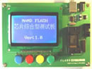
NAND FLASHоƬ�ۺϲ���(��Ƭ) NAND FLASHоƬ�ۺϲ����п�Ժ�����������Ƶ���Ƽ���չ��˾���ƣ��Զ�ʶ����Ʒ�Ƶ�NAND FLASHоƬ��Ʒ�����ơ�ԭ���ͺš�������������ɾ��������ͬʱ���Ի�������������0�����ر���ʾ������ص���ǿ��Բ���оƬ��д���ٶȣ����ȴﵽ10uS��ȷ�жϱ�����оƬ�ĵȼ��� ����������������������оƬɾ������ʾ����������������˲��ʶ���û��LOGO�İ�Ƭ��ԭ��Ʒ�����ƺ��ͺ��������ǿ��С��������ɹ��ж�оƬ���ӣ�ʶ���Ƭ�ͼ�ð��ĥƬ���������ߡ�������չ1-7���������壬ʵ�ֶ�Ƭͬʱ���ԡ�ɾ����COPY�� ��������:http://www.cherrychip.net/FLASH-T1.pdf * - ���������ʱ�䣺2006-7-15 14:02:24 ���ߣ�cherrychip
|
|
| 47¥�� | >>�������� |
| ���ߣ� ���� �� 2006/7/14 10:04:00 ������
���� û������ |
|
| 48¥�� | >>�������� |
| ���ߣ� nichao99 �� 2006/7/18 11:42:00 ������
�������� |
|
| 49¥�� | >>�������� |
| ���ߣ� gxpa1 �� 2006/9/12 9:58:00 ������
���� |
|
| 50¥�� | >>�������� |
| ���ߣ� ��չ�Ƽ� �� 2006/9/20 10:19:00 ������
���������� ���������� |
|
| 51¥�� | >>�������� |
| ���ߣ� honeir �� 2006/9/29 19:07:00 ������
Thanks a lot! ¥���ܷ�һ�ݸ��ң������e�ĵ�һ�鷢���ң� лл�� |
|
| 52¥�� | >>�������� |
| ���ߣ� bjjtyl �� 2006/10/14 22:07:00 ������
�ܷ�������ϸ��ҷ�һ�ݣ� �ܷ�������ϸ��ҷ�һ�ݣ�лл����Ҳѧϰѧϰ�� ��ӭ�� |
|
| 53¥�� | >>�������� |
| ���ߣ� shaohaigod �� 2006/10/30 18:07:00 ������
����һ�ݰ� ����һ�ݰ� shaohaigod@163.com |
|
| 54¥�� | >>�������� |
| ���ߣ� micheal123 �� 2006/11/9 14:20:00 ������
thanks |
|
| 55¥�� | >>�������� |
| ���ߣ� gliu �� 2006/11/15 17:02:00 ������
3Q ���¥�������ĵĻ�,�Ǿ��ֵ��ҷ�һ���� lg_vagrant@163.com |
|
| 56¥�� | >>�������� |
| ���ߣ� lhmail3 �� 2006/12/11 14:32:00 ������
�ð� �ð� |
|
| 57¥�� | >>�������� |
| ���ߣ� qiang0726 �� 2007/1/9 14:21:00 ������
лл |
|
| 58¥�� | >>�������� |
| ���ߣ� kings8105 �� 2007/1/27 12:58:00 ������
��Ҫ! �Ǻ�~~ ��Ҳ��Ҫһ�� �ҵ�E-MAIL:kings8105@hotmail.com лл! |
|
| 59¥�� | >>�������� |
| ���ߣ� 9805210005 �� 2007/2/28 17:01:00 ������
����Ҫһ�� �Һ���Ҫ��wang.zi.ling@163.com ��л�� |
|
| 60¥�� | >>�������� |
| ���ߣ� devil110 �� 2007/3/7 10:22:00 ������
����û��Ŷ! ���еĻ�����һ��Ŷ!:devil5_angel!163.com лл��! |
|
| 61¥�� | >>�������� |
| ���ߣ� ha_exit �� 2007/3/13 21:02:00 ������
�ö��� ���ʣ���ô�������������Ӱ� |
|
| 62¥�� | >>�������� |
| ���ߣ� �������� �� 2007/3/20 21:55:00 ������
�������أ� �������أ� |
|
| 63¥�� | >>�������� |
| ���ߣ� xuqinglei �� 2007/3/26 16:39:00 ������
where? ���أ� |
|
| 64¥�� | >>�������� |
| ���ߣ� budoudou �� 2007/4/19 9:56:00 ������
�ð� ��Ҳ��Ҫһ�ݣ���ллѽ���� |
|
| 65¥�� | >>�������� |
| ���ߣ� phton �� 2007/5/10 16:38:00 ������
LZ���� |
|
| 66¥�� | >>�������� |
| ���ߣ� kathleen �� 2008/10/5 22:06:47 ������
¥�����ɷ����һ�ݰ���ллŶ |
|
|
|
| ���ע��Ϊά����ӿ�������Ա��������ӹ���ʦ�������ۣ���˽��� |
Copyright © 1998-2006 www.dzsc.com ��ICP֤030469�� |