鈥?/div>
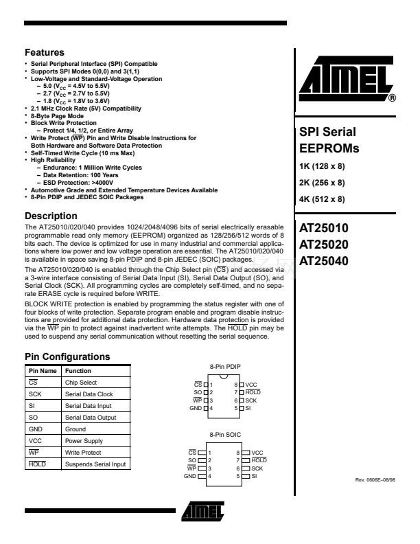
Description
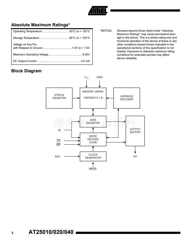
The AT25010/020/040 provides 1024/2048/4096 bits of serial electrically erasable
programmable read only memory (EEPROM) organized as 128/256/512 words of 8
bits each. The device is optimized for use in many industrial and commercial applica-
tions where low power and low voltage operation are essential. The AT25010/020/040
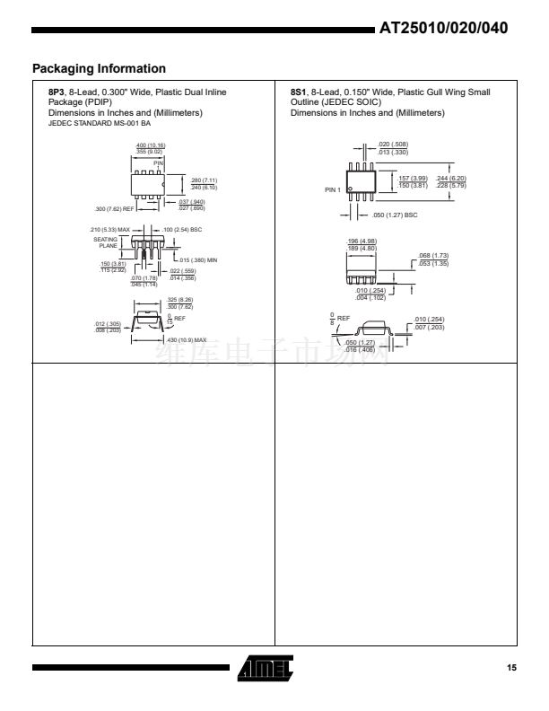
is available in space saving 8-pin PDIP and 8-pin JEDEC (SOIC) packages.
The AT25010/020/040 is enabled through the Chip Select pin (CS) and accessed via
a 3-wire interface consisting of Serial Data Input (SI), Serial Data Output (SO), and
Serial Clock (SCK). All programming cycles are completely self-timed, and no sepa-
rate ERASE cycle is required before WRITE.
BLOCK WRITE protection is enabled by programming the status register with one of
four blocks of write protection. Separate program enable and program disable instruc-
tions are provided for additional data protection. Hardware data protection is provided
via the WP pin to protect against inadvertent write attempts. The HOLD pin may be
used to suspend any serial communication without resetting the serial sequence.
AT25010
AT25020
AT25040
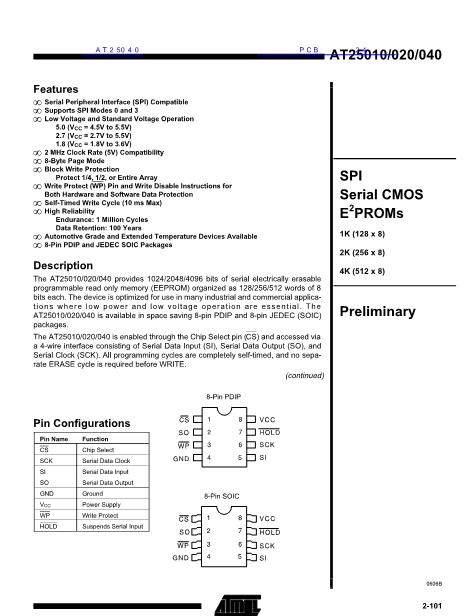
Pin Configurations
Pin Name
CS
SCK
SI
SO
GND
VCC
WP
HOLD
Function
Chip Select
Serial Data Clock
Serial Data Input
Serial Data Output
Ground
Power Supply
Write Protect
Suspends Serial Input
CS
SO
WP
GND
1
2
3
4
8
7
6
5
VCC
HOLD
SCK
SI
CS
SO
WP
GND
8-Pin PDIP
1
2
3
4
8
7
6
5
VCC
HOLD
SCK
SI
SPI, 1K Serial
E
2
PROM
8-Pin SOIC
Rev. 0606E鈥?8/98
1


 1
1
 2
2
 3
3
 4
4
 5
5
 6
6
 7
7
 8
8
 9
9
 10
10
 11
11
 12
12
 13
13
 14
14
 15
15
