鈥?/div>
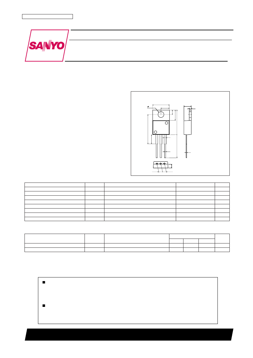
Package Dimensions
unit : mm
2010C
[2SB1683 / 2SD2639]
10.2
3.6
5.1
2.7
6.3
4.5
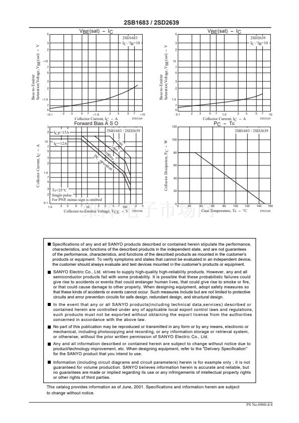
Wide ASO because of on-chip ballast resistance.
Good dependence of fT on current and good HF
characteristic.
1.3
18.0
5.6
1.2
14.0
0.8
15.1
0.4
1 2 3
2.7
Specifications
( ) : 2SB1683
Absolute Maximum Ratings
at Ta=25掳C
Parameter
Collector-to-Base Voltage
Collector-to-Emitter Voltage
Emitter-to-Base Voltage
Collector Current
Collector Current (Pulse)
Collector Dissipation
Junction Temperature
Storage Temperature
Symbol
VCBO
VCEO
VEBO
IC
ICP
PC
Tj
Tstg
Conditions
2.55
1 : Base
2 : Collector
3 : Emitter
2.55
SANYO : TO-220
Ratings
(--)160
(--)140
(--)6
(--)12
(--)15
80
150
--40 to +150
Tc=25掳C
Unit
V
V
V
A
A
W
掳C
掳C
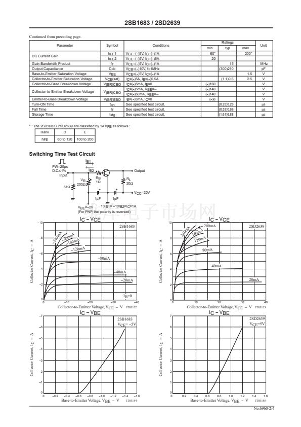
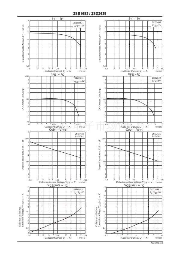
Electrical Characteristics
at Ta=25掳C
Parameter
Collector Cutoff Current
Emitter Cutoff Current
Symbol
ICBO
IEBO
Conditions
VCB=(--)80V, IE=0
VEB=(--)4V, IC=0
Ratings
min
typ
max
(--)0.1
(--)0.1
Unit
mA
mA
Continued on next page.
Any and all SANYO products described or contained herein do not have specifications that can handle
applications that require extremely high levels of reliability, such as life-support systems, aircraft's
control systems, or other applications whose failure can be reasonably expected to result in serious
physical and/or material damage. Consult with your SANYO representative nearest you before using
any SANYO products described or contained herein in such applications.
SANYO assumes no responsibility for equipment failures that result from using products at values that
exceed, even momentarily, rated values (such as maximum ratings, operating condition ranges, or other
parameters) listed in products specifications of any and all SANYO products described or contained
herein.
SANYO Electric Co.,Ltd. Semiconductor Company
TOKYO OFFICE Tokyo Bldg., 1-10, 1 Chome, Ueno, Taito-ku, TOKYO, 110-8534 JAPAN
62501 TS IM TA-3139, 3140 No.6960-1/4


 1
1
 2
2
 3
3
 4
4
