PRELIMINARY DATA SHEET
SILICON TRANSISTOR
2SC5433
NPN EPITAXIAL SILICON TRANSISTOR
FOR HIGH-FREQUENCY LOW-NOISE AMPLIFICATION
FEATURE
鈥?Ultra super mini-mold thin flat package
(1.4 mm
脳
0.8 mm
脳
0.59 mm: TYP.)
鈥?Contains same chip as 2SC5007
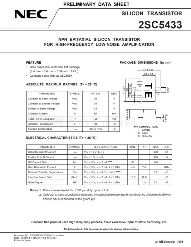
PACKAGE DIMENSIONS (in mm)
1.4 卤 0.05
0.8 卤 0.1
1.4 卤 0.1
(0.9)
0.45 0.45
0.2
+0.1
鈥?
ABSOLUTE MAXIMUM RATINGS (T
A
= 25
掳
C)
PARAMETER
Collector to Base Voltage
Collector to Emitter Voltage
Emitter to Base Voltage
Collector Current
Total Power Dissipation
Junction Temperature
Storage Temperature
SYMBOL
V
CBO
V
CEO
V
EBO
I
C
P
T
T
j
T
stg
RATING
20
10
1.5
65
125
150
鈥?5 to +150
UNIT
V
V
TE
3
1
mW
掳C
掳C
ELECTRICAL CHARACTERISTICS (T
A
= 25
掳
C)
PARAMETER
Collector Cut-off Current
Emitter Cut-off Current
DC Current Gain
Gain Bandwidth Product
Reverse Transfer Capacitance
Insertion Power Gain
Noise Figure
SYMBOL
I
CBO
I
EBO
h
FE
f
T
Cre
|S
21e
|
2
NF
TEST CONDITIONS
V
CB
= 10 V, I
E
= 0
V
EB
= 1 V, I
C
= 0
V
CE
= 3 V, I
C
= 7 mA
Note 1
V
CE
= 3 V, I
C
= 7 mA, f = 1 GHz
V
CB
= 3 V, I
E
= 0, f = 1 MHz
Note 2
V
CE
= 3 V, I
C
= 7 mA, f = 1 GHz
V
CE
= 3 V, I
C
= 7 mA, f = 1 GHz
PIN CONNECTIONS
1: Emitter
2: Base
3: Collector
MIN.
TYP.
MAX.
800
800
UNIT
nA
nA
80
4.5
7.0
145
GHz
0.9
pF
dB
2.7
dB
10.0
12.0
1.4
Notes 1.
Pulse measurement P
W
鈮?/div>
350
碌
s, duty cycle
鈮?/div>
2 %
2.
Collector to base capacitance measured by capacitance meter (automatic balance bridge method) when
emitter pin is connected to the guard pin.
Because this product uses high-frequency process, avoid excessive input of static electricity, etc.
The information in this document is subject to change without notice.
Document No. P13077EJ1V0DS00 (1st edition)
Date Published February 1998 N CP(K)
Printed in Japan
漏
0.15
+0.1
鈥?.05
mA
0.59 卤 0.05
V
0.3
+0.1
鈥?
2
1998


 1
1
 2
2
 3
3
 4
4
 5
5
 6
6
 7
7
 8
8
