鈩?/div>
(typ.)
High forward transfer admittance: |Y
fs
| = 4.3 S (typ.)
Low leakage current: I
DSS
=
100
碌A (max) (V
DS
= 450 V)
Enhancement-model: V
th
= 3.0~5.0 V (V
DS
=
10
V, I
D
=
1
mA)
路
路
路
路
Maximum Ratings
(Ta
=
25掳C)
Characteristics
Drain-source voltage
Drain-gate voltage (R
GS
=
20 kW)
Gate-source voltage
Drain current
DC
Pulse
(Note 1)
(Note 1)
Symbol
V
DSS
V
DGR
V
GSS
I
D
I
DP
P
D
E
AR
I
AR
E
AR
T
ch
T
stg
Rating
450
450
卤30
10
40
40
222
10
4
150
-55~150
Unit
V
V
V
A
W
mJ
A
mJ
掳C
掳C
Drain power dissipation (Tc
=
25掳C)
Single pulse avalanche energy
(Note 2)
Avalanche current
Repetitive avalanche energy (Note 3)
Channel temperature
Storage temperature range
JEDEC
JEITA
TOSHIBA
鈥?/div>
SC-67
2-10R1B
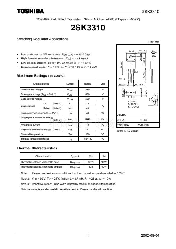
Weight: 1.9 g (typ.)
Thermal Characteristics
Characteristics
Thermal resistance, channel to case
Thermal resistance, channel to ambient
Symbol
R
th (ch-c)
R
th (ch-a)
Max
3.125
62.5
Unit
掳C/W
掳C/W
Note 1: Please use devices on conditions that the channel temperature is below 150掳C.
Note 2: V
DD
=
90 V, T
ch
=
25掳C (initial), L
=
3.7 mH, R
G
=
25
W,
I
AR
=
10 A
Note 3: Repetitive rating: Pulse width limited by maximum channel temperature
This transistor is an electrostatic sensitive device. Please handle with caution.
1
2002-09-04


 1
1
 2
2
 3
3
 4
4
 5
5
 6
6
