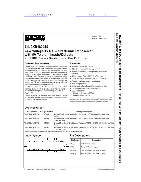
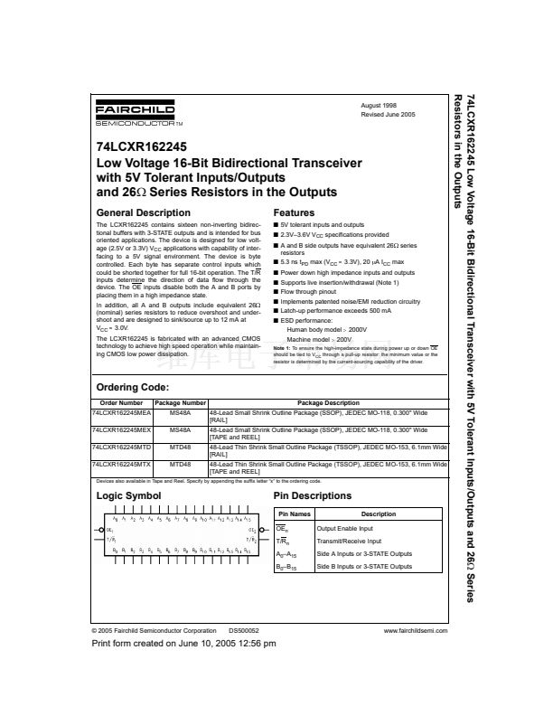
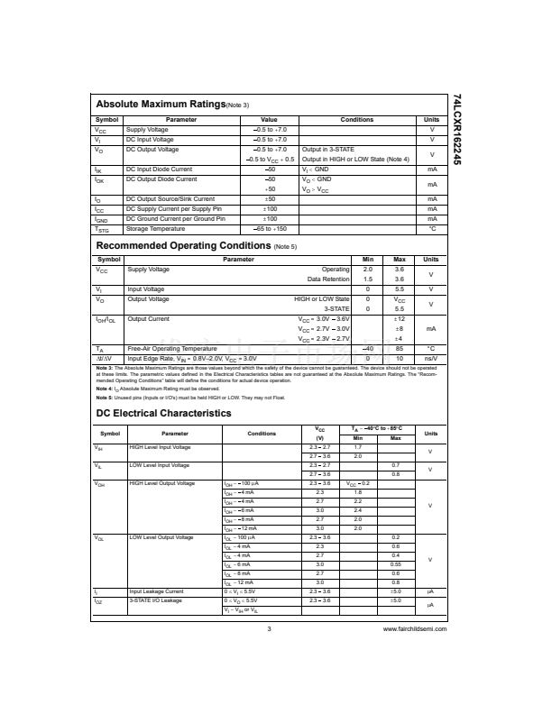
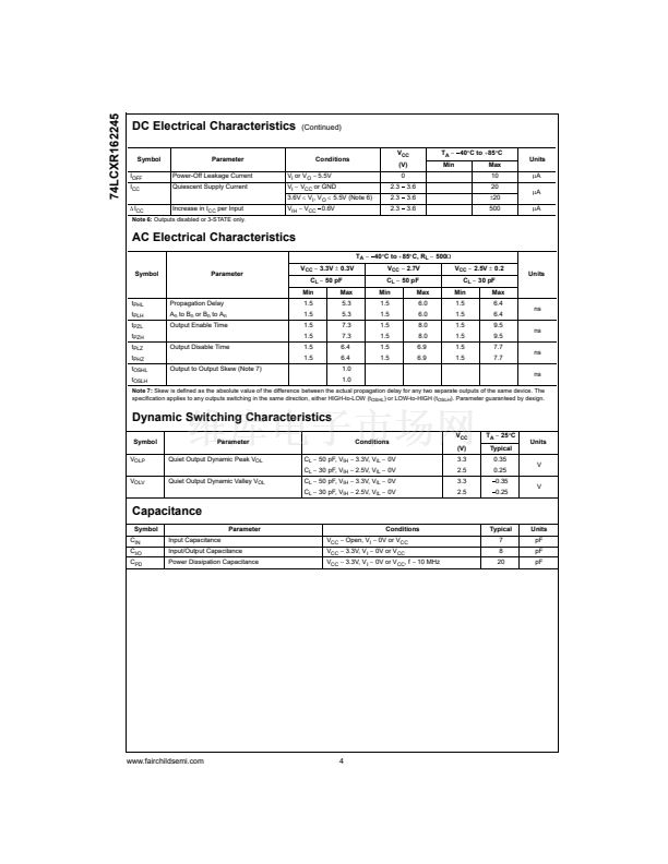
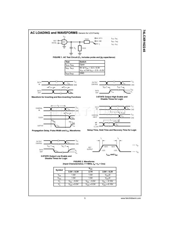
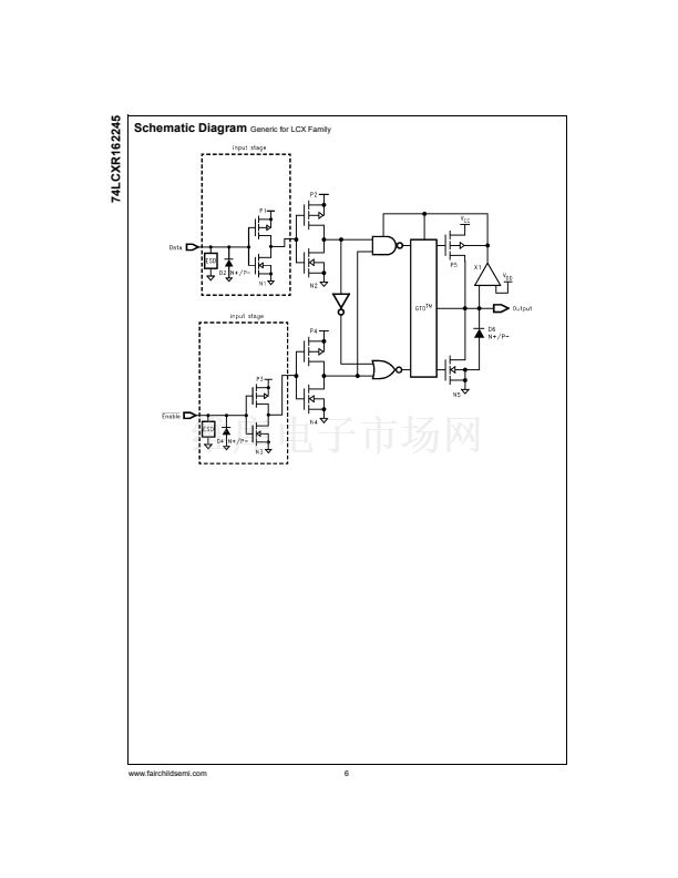
74LCXR162245 Low Voltage 16-Bit Bidirectional Transceiver with 5V Tolerant Inputs/Outputs and 26: Series
Resistors in the Outputs
August 1998
Revised June 2005
74LCXR162245
Low Voltage 16-Bit Bidirectional Transceiver
with 5V Tolerant Inputs/Outputs
and 26: Series Resistors in the Outputs
General Description
The LCXR162245 contains sixteen non-inverting bidirec-
tional buffers with 3-STATE outputs and is intended for bus
oriented applications. The device is designed for low volt-
age (2.5V or 3.3V) V
CC
applications with capability of inter-
facing to a 5V signal environment. The device is byte
controlled. Each byte has separate control inputs which
could be shorted together for full 16-bit operation. The T/R
inputs determine the direction of data flow through the
device. The OE inputs disable both the A and B ports by
placing them in a high impedance state.
In addition, all A and B outputs include equivalent 26
:
(nominal) series resistors to reduce overshoot and under-
shoot and are designed to sink/source up to 12 mA at
V
CC
3.0V.
The LCXR162245 is fabricated with an advanced CMOS
technology to achieve high speed operation while maintain-
ing CMOS low power dissipation.
Features
s
5V tolerant inputs and outputs
s
2.3V鈥?.6V V
CC
specifications provided
s
A and B side outputs have equivalent 26
:
series
resistors
s
5.3 ns t
PD
max (V
CC
3.3V), 20
P
A I
CC
max
s
Power down high impedance inputs and outputs
s
Supports live insertion/withdrawal (Note 1)
s
Flow through pinout
s
Implements patented noise/EMI reduction circuitry
s
Latch-up performance exceeds 500 mA
s
ESD performance:
Human body model
!
2000V
Machine model
!
200V
Note 1:
To ensure the high-impedance state during power up or down OE
should be tied to V
CC
through a pull-up resistor: the minimum value or the
resistor is determined by the current-sourcing capability of the driver.
Ordering Code:
Order Number
74LCXR162245MEA
74LCXR162245MEX
74LCXR162245MTD
74LCXR162245MTX
Package Number
MS48A
MS48A
MTD48
MTD48
Package Description
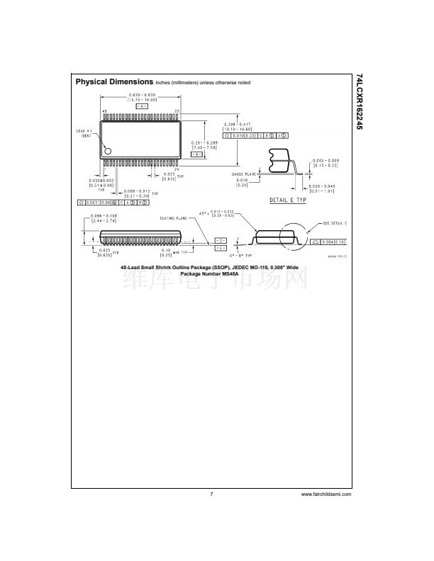
48-Lead Small Shrink Outline Package (SSOP), JEDEC MO-118, 0.300" Wide
[RAIL]
48-Lead Small Shrink Outline Package (SSOP), JEDEC MO-118, 0.300" Wide
[TAPE and REEL]
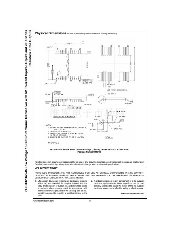
48-Lead Thin Shrink Small Outline Package (TSSOP), JEDEC MO-153, 6.1mm Wide
[RAIL]
48-Lead Thin Shrink Small Outline Package (TSSOP), JEDEC MO-153, 6.1mm Wide
[TAPE and REEL]
Devices also available in Tape and Reel. Specify by appending the suffix letter 鈥渪鈥?to the ordering code.
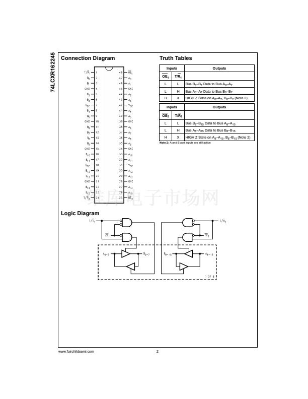
Logic Symbol
Pin Descriptions
Pin Names
OE
n
T/R
n
A
0
鈥揂
15
B
0
鈥揃
15
Description
Output Enable Input
Transmit/Receive Input
Side A Inputs or 3-STATE Outputs
Side B Inputs or 3-STATE Outputs
漏 2005 Fairchild Semiconductor Corporation
DS500052
www.fairchildsemi.com
Print form created on June 10, 2005 12:56 pm


 1
1
 2
2
 3
3
 4
4
 5
5
 6
6
 7
7
 8
8
