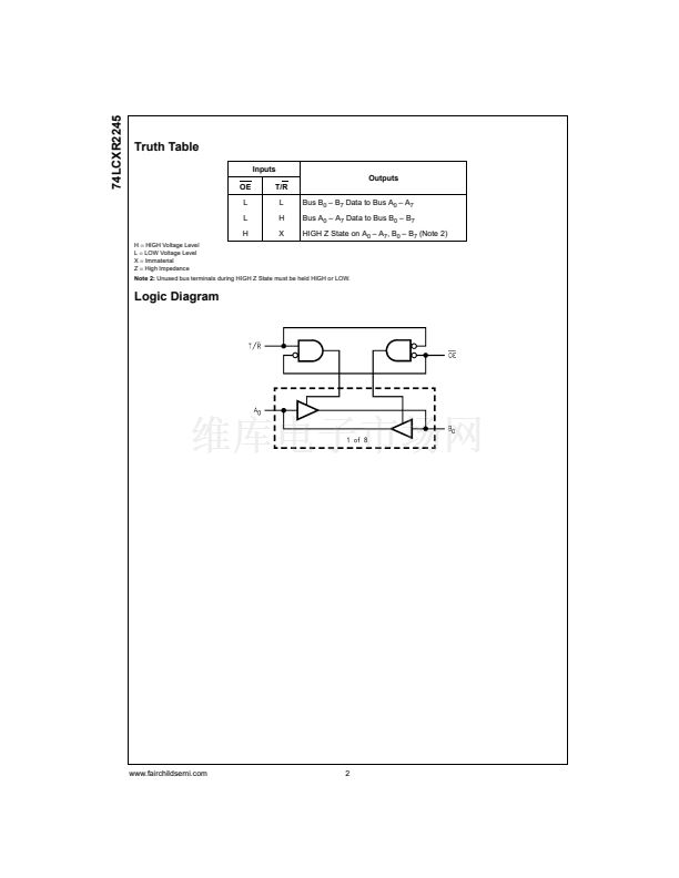
ented applications. The device is designed for low voltage
ing to a 5V signal environment. The T/R input determines
the direction of data flow through the device. The OE input
impedance state. The 26
鈩?/div>
series resistor helps reduce
output overshoot and undershoot.
The LCXR2245 is fabricated with an advanced CMOS
technology to achieve high speed operation while maintain-
ing CMOS low power dissipation.
Features
s
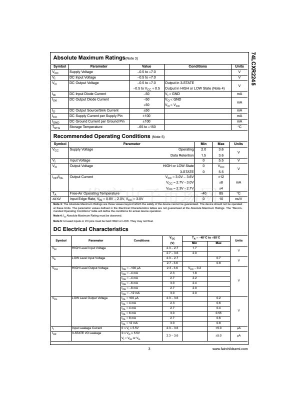
5V tolerant inputs and outputs
s
2.3V鈥?.6V V
CC
specifications provided
s
8.0 ns t
PD
max (V
CC
=
3.3V), 10
碌
A I
CC
max
s
Power down high impedance inputs and outputs
s
Supports live insertion/withdrawal (Note 1)
s
卤
12 mA output drive (V
CC
=
3.0V)
s
Implements patented noise/EMI reduction circuitry
s
Latch-up performance exceeds 500 mA
s
Equivalent 26
鈩?/div>
series resistor on all outputs
s
ESD performance:
Human body model
>
2000V
Machine model
>
200V
Note 1:
To ensure the high-impedance state during power up or down, OE
should be tied to V
CC
through a pull-up resistor: the minimum value or the
resistor is determined by the current-sourcing capability of the driver.
Ordering Code:
Order Number
74LCXR2245WM
74LCXR2245SJ
74LCXR2245MSA
74LCXR2245MTC
Package Number
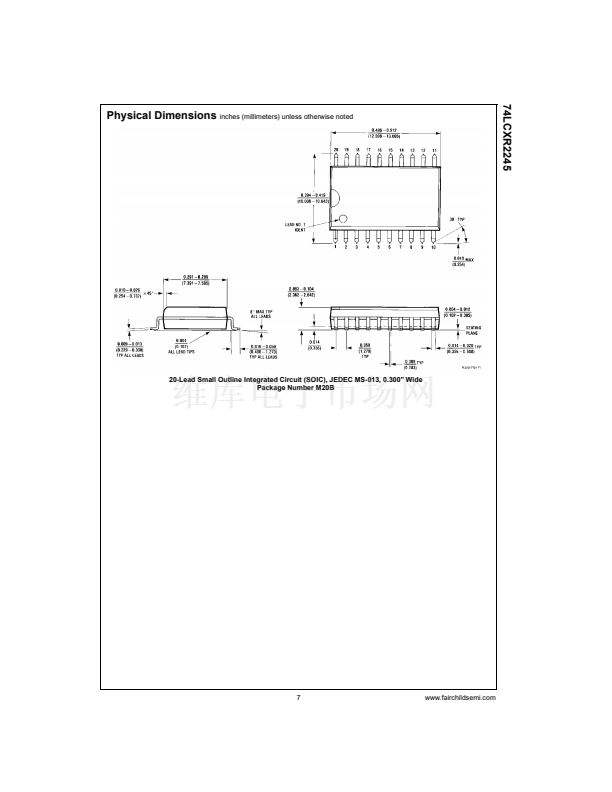
M20B
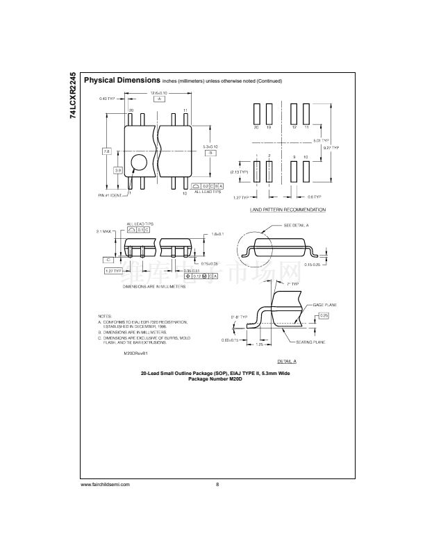
M20D
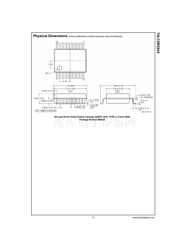
MSA20
MTC20
Package Description
20-Lead Small Outline Integrated Circuit (SOIC), JEDEC MS-013, 0.300" Wide
20-Lead Small Outline Package (SOP), EIAJ TYPE II, 5.3mm Wide
20-Lead Shrink Small Outline Package (SSOP), EIAJ TYPE II, 5.3mm Wide
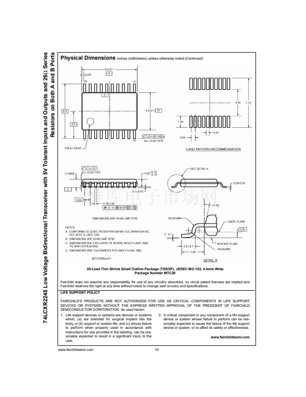
20-Lead Thin Shrink Small Outline Package (TSSOP), JEDEC MO-153, 4.4mm Wide
Devices also available in Tape and Reel. Specify by appending the suffix letter 鈥淴鈥?to the ordering code.
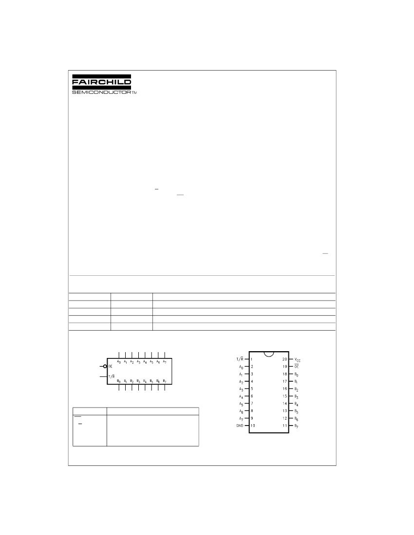
Logic Symbol
Connection Diagram
Pin Descriptions
Pin Names
OE
T/R
A
0
鈥揂
7
B
0
鈥揃
7
Description
Output Enable Input
Transmit/Receive Input
Side A Inputs or 3-STATE Outputs
Side B Inputs or 3-STATE Outputs
漏 2000 Fairchild Semiconductor Corporation
DS500361
www.fairchildsemi.com


 1
1
 2
2
 3
3
 4
4
 5
5
 6
6
 7
7
 8
8
 9
9
 10
10
