Ultrafast SiGe
Voltage Comparators
ADCMP580/ADCMP581/ADCMP582
FEATURES
180 ps propagation delay
25 ps overdrive and slew rate dispersion
8 GHz equivalent input rise time bandwidth
100 ps minimum pulse width
37 ps typical output rise/fall
10 ps deterministic jitter (DJ)
200 fs random jitter (RJ)
鈭?
V to +3 V input range with +5 V/鈭? V supplies
On-chip terminations at both input pins
Resistor-programmable hysteresis
Differential latch control
Power supply rejection > 70 dB
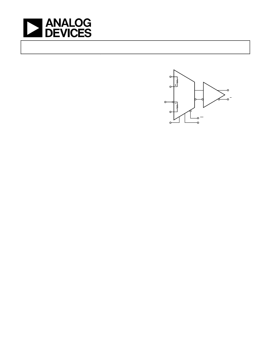
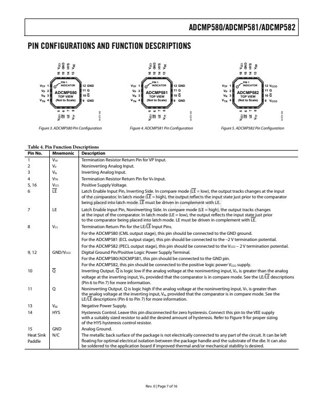
FUNCTIONAL BLOCK DIAGRAM
V
TP
TERMINATION
V
P
NONINVERTING
INPUT
V
N
INVERTING
INPUT
V
TN
TERMINATION
ADCMP580/
ADCMP581/
ADCMP582
Q OUTPUT
CML/ECL/
PECL
Q OUTPUT
LE INPUT
HYS
LE INPUT
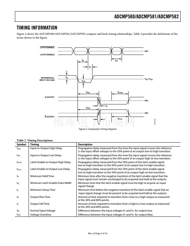
Figure 1.
APPLICATIONS
Automatic test equipment (ATE)
High speed instrumentation
Pulse spectroscopy
Medical imaging and diagnostics
High speed line receivers
Threshold detection
Peak and zero-crossing detectors
High speed trigger circuitry
Clock and data signal restoration
GENERAL DESCRIPTION
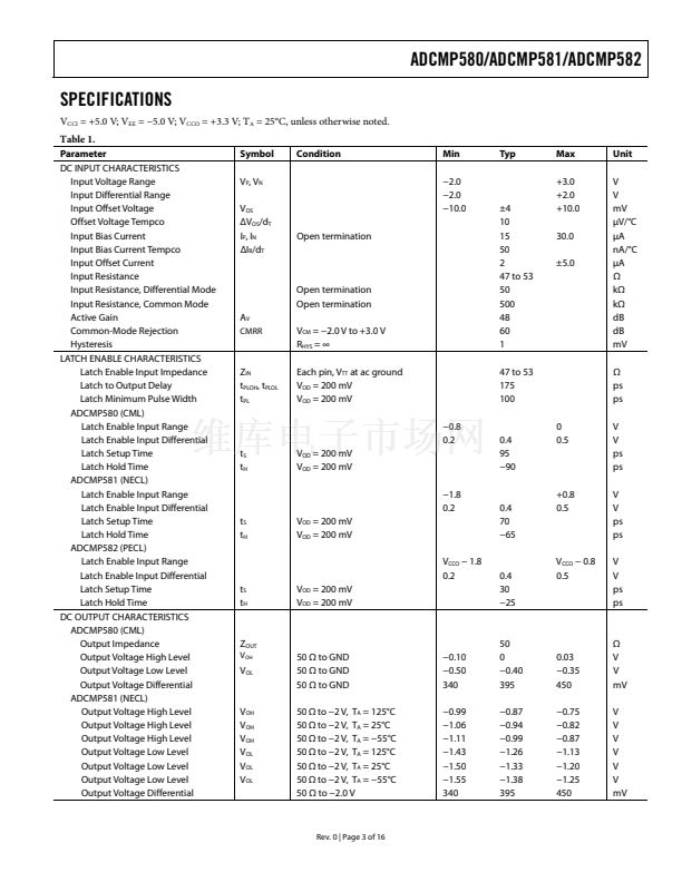
The ADCMP580/ADCMP581/ADCMP582 are ultrafast voltage
comparators fabricated on Analog Devices鈥?proprietary XFCB3
Silicon Germanium (SiGe) bipolar process. The ADCMP580
features CML output drivers; the ADCMP581 features reduced
swing ECL (negative ECL) output drivers; and the ADCMP582
features reduced swing PECL (positive ECL) output drivers.
All three comparators offer 180 ps propagation delay and
100 ps minimum pulse width for 10 Gbps operation with
200 fs random jitter (RJ). Overdrive and slew rate dispersion
are typically less than 15 ps.
The 卤5 V power supplies enable a wide
鈭?
V to +3 V input
range with logic levels referenced to the CML/NECL/PECL
outputs. The inputs have 50 惟 on-chip termination resistors
with the optional capability to be left open (on an individual
pin basis) for applications requiring high impedance input.
The CML output stage is designed to directly drive 400 mV
into 50 惟 transmission lines terminated to ground. The NECL
output stages are designed to directly drive 400 mV into 50 惟
terminated to
鈭?
V. The PECL output stages are designed to
directly drive 400 mV into 50 惟 terminated to V
CCO
鈭?/div>
2 V.
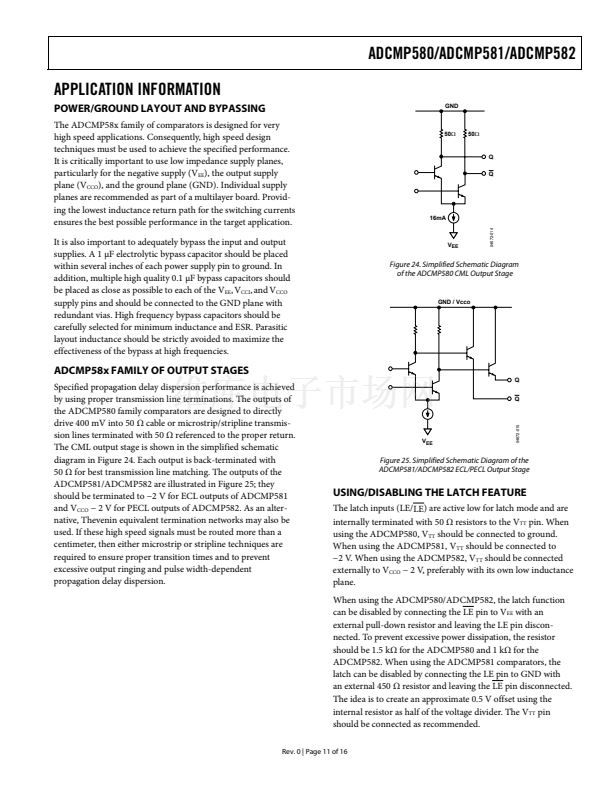
High speed latch and programmable hysteresis are also
provided. The differential latch input controls are also 50 惟
terminated to an independent V
TT
pin to interface to either
CML or ECL or to PECL logic.
The ADCMP580/ADCMP581/ADCMP582 are available in
a 16-lead LFCSP package.
Rev. 0
Information furnished by Analog Devices is believed to be accurate and reliable. However, no
responsibility is assumed by Analog Devices for its use, nor for any infringements of patents or other
rights of third parties that may result from its use. Specifications subject to change without notice. No
license is granted by implication or otherwise under any patent or patent rights of Analog Devices.
Trademarks and registered trademarks are the property of their respective owners.
One Technology Way, P.O. Box 9106, Norwood, MA 02062-9106, U.S.A.
Tel: 781.329.4700
www.analog.com
Fax: 781.461.3113
漏 2005 Analog Devices, Inc. All rights reserved.
04672-001


 1
1
 2
2
 3
3
 4
4
 5
5
 6
6
 7
7
 8
8
 9
9
 10
10
 11
11
 12
12
 13
13
 14
14
 15
15
 16
16
