C4鈥?/div>
C4
1碌F
VOLTAGE
SHUTDOWN DISCHARGE INVERTER
CONTROL
GND
鈥?0.2V
C9
1碌F
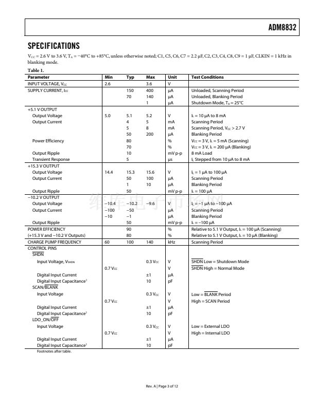
Figure 1.
GENERAL DESCRIPTION
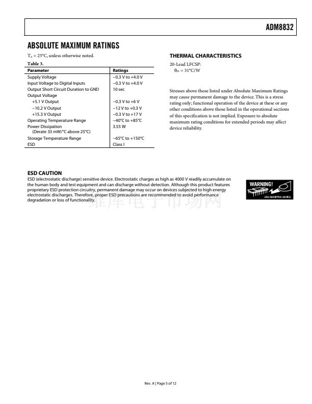
The ADM8832 is a charge pump regulator used for color thin
film transistor (TFT) liquid crystal displays (LCD). Using charge
pump technology, the device can be used to generate three
output voltages (+5.1 V 卤2%, +15.3 V, 鈭?0.2 V) from a single
3 V input supply. These outputs are then used to provide
supplies for the LCD controller (+5.1 V) and the gate drives for
the transistors in the panel (+15.3 V and 鈭?0.2 V). Only a few
external capacitors are needed for the charge pumps. An
efficient low dropout voltage regulator also ensures that the
power efficiency is high and provides a low ripple 5.1 V output.
This LDO can be shut down and an external LDO used to
regulate the 5 V doubler output and drive the input to the
charge pump section, which generates the +15.3 V and 鈭?0.2 V
outputs if so required by the user.
The ADM8832 has an internal 100 kHz oscillator for use in
scanning mode, but the part must be clocked by an external
clock source in blanking (low current) mode. The internal
oscillator is used to clock the charge pumps during scanning
mode where the current is highest. During blanking periods, the
ADM8832 switches to an external, lower frequency clock. This
allows the user to vary the frequency and maximize power
efficiency during blanking periods. The tolerances on the output
voltages are seamlessly maintained when switching from scan-
ning mode to blanking mode or vice versa.
The ADM8832 power saving features include low power
shutdown and reduced quiescent current consumption during
the blanking periods. The 5.1 V output consumes the most
power, so power efficiency is also maximized on this output
with an oscillator enabling scheme (Green Idle鈩?. This
effectively senses the load current that is flowing and turns on
the charge pump only when charge needs to be delivered to the
5 V pump doubler output.
The ADM8832 is fabricated using CMOS technology for minimal
power consumption. The part is packaged in a 20-lead LFCSP
(lead frame chip scale package).
Rev. A
Information furnished by Analog Devices is believed to be accurate and reliable.
However, no responsibility is assumed by Analog Devices for its use, nor for any
infringements of patents or other rights of third parties that may result from its use.
Specifications subject to change without notice. No license is granted by implication
or otherwise under any patent or patent rights of Analog Devices. Trademarks and
registered trademarks are the property of their respective owners.
One Technology Way, P.O. Box 9106, Norwood, MA 02062-9106, U.S.A.
Tel: 781.329.4700
www.analog.com
Fax: 781.326.8703
漏 2004 Analog Devices, Inc. All rights reserved.
03759-A-001
鈥?0VOUT


 1
1
 2
2
 3
3
 4
4
 5
5
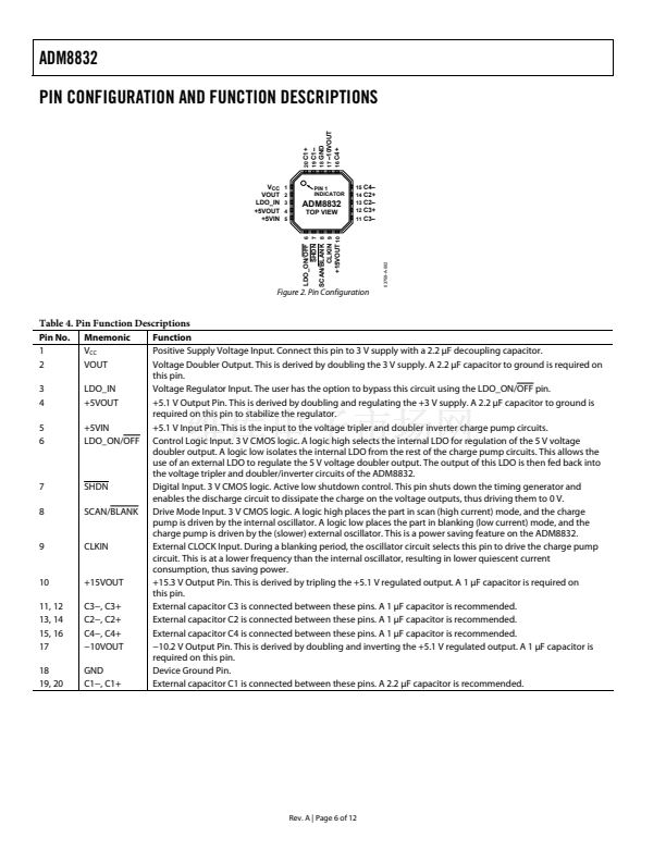 6
6
 7
7
 8
8
 9
9
 10
10
 11
11
 12
12
