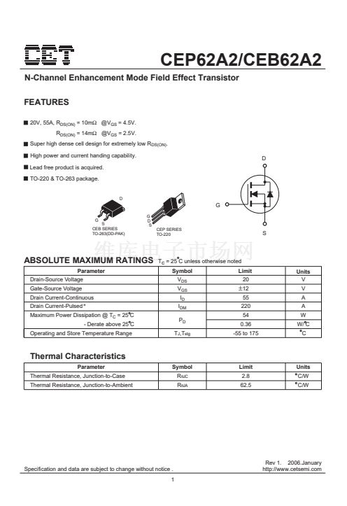
CEP62A2/CEB62A2
N-Channel Enhancement Mode Field Effect Transistor
FEATURES
20V, 55A, R
DS(ON)
= 10m鈩?@V
GS
= 4.5V.
R
DS(ON)
= 14m鈩?@V
GS
= 2.5V.
Super high dense cell design for extremely low R
DS(ON)
.
High power and current handing capability.
Lead free product is acquired.
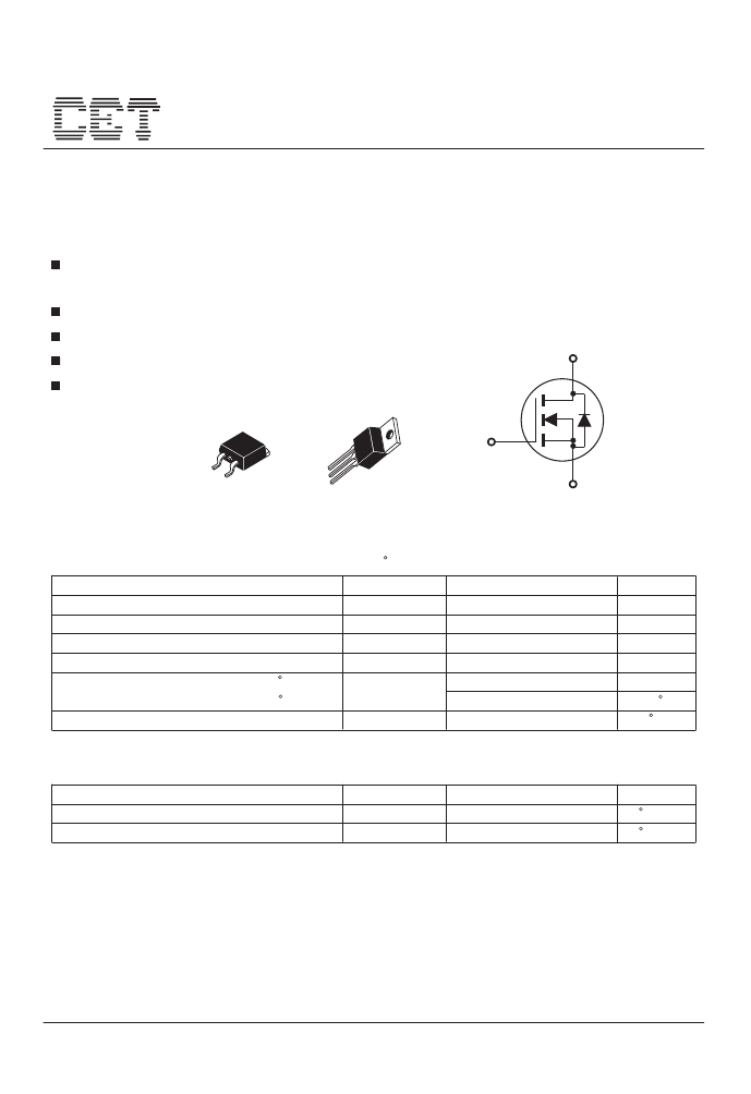
TO-220 & TO-263 package.
D
D
G
S
CEB SERIES
TO-263(DD-PAK)
G
G
D
S
CEP SERIES
TO-220
S
ABSOLUTE MAXIMUM RATINGS
Parameter
Drain-Source Voltage
Gate-Source Voltage
Drain Current-Continuous
Drain Current-Pulsed
a
Tc = 25 C unless otherwise noted
Symbol
V
DS
V
GS
I
D
I
DM
P
D
T
J
,T
stg
Limit
20
Units
V
V
A
A
W
W/ C
C
卤
12
55
220
54
0.36
-55 to 175
Maximum Power Dissipation @ T
C
= 25 C
- Derate above 25 C
Operating and Store Temperature Range
Thermal Characteristics
Parameter
Thermal Resistance, Junction-to-Case
Thermal Resistance, Junction-to-Ambient
Symbol
R
胃JC
R
胃JA
Limit
2.8
62.5
Units
C/W
C/W
Specification and data are subject to change without notice .
1
Rev 1. 2006.January
http://www.cetsemi.com


 1
1
 2
2
 3
3
 4
4
