DM74LS165 8-Bit Parallel In/Serial Output Shift Registers
August 1986
Revised March 2000
DM74LS165
8-Bit Parallel In/Serial Output Shift Registers
General Description
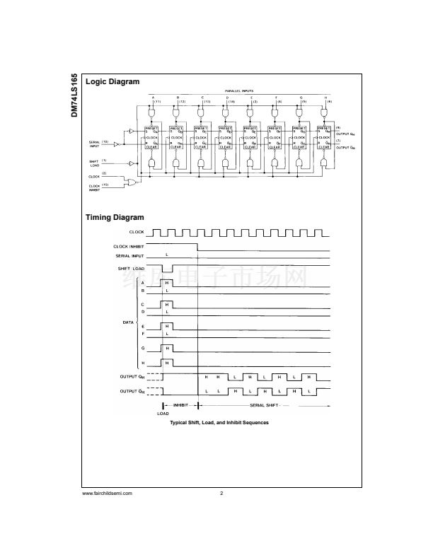
This device is an 8-bit serial shift register which shifts data
in the direction of Q
A
toward Q
H
when clocked. Parallel-in
access is made available by eight individual direct data
inputs, which are enabled by a low level at the shift/load
input. These registers also feature gated clock inputs and
complementary outputs from the eighth bit.
Clocking is accomplished through a 2-input NOR gate, per-
mitting one input to be used as a clock-inhibit function.
Holding either of the clock inputs HIGH inhibits clocking,
and holding either clock input LOW with the load input
HIGH enables the other clock input. The clock-inhibit input
should be changed to the high level only while the clock
input is HIGH. Parallel loading is inhibited as long as the
load input is HIGH. Data at the parallel inputs are loaded
directly into the register on a HIGH-to-LOW transition of the
shift/load input, regardless of the logic levels on the clock,
clock inhibit, or serial inputs.
Features
s
Complementary outputs
s
Direct overriding (data) inputs
s
Gated clock inputs
s
Parallel-to-serial data conversion
s
Typical frequency 35 MHz
s
Typical power dissipation 105 mW
Ordering Code:
Order Number
DM74LS165M
DM74LS165WM
DM74LS165N
Package Number
M16A
M16B
N16E
Package Description
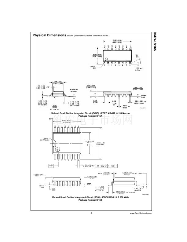
16-Lead Small Outline Integrated Circuit (SOIC), JEDEC MS-012, 0.150 Narrow
16-Lead Small Outline Intergrated Circuit (SOIC), JEDEC MS-013, 0.300 Wide
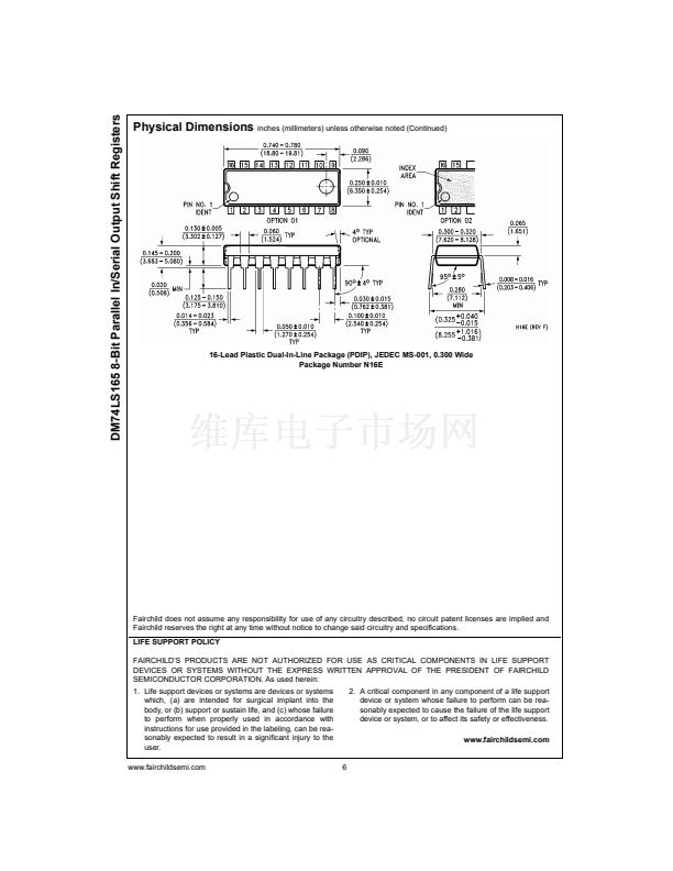
16-Lead Plastic Dual-In-Line Package (PDIP), JEDEC MS-001, 0.300 Wide
Devices also available in Tape and Reel. Specify by appending the suffix letter 鈥淴鈥?to the ordering code.
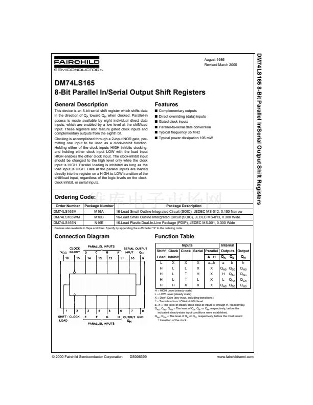
Connection Diagram
Function Table
Inputs
Load Inhibit
L
H
H
H
H
X
L
L
L
H
X
L
鈫?/div>
鈫?/div>
X
X
X
H
L
X
A...H
a...h
X
X
X
X
Internal
Q
A
a
H
L
Q
B
b
Q
An
Q
An
Q
H
h
Q
H0
Q
Gn
Q
Gn
Q
H0
Shift/ Clock Clock Serial Parallel Outputs Output
Q
A0
Q
B0
Q
A0
Q
B0
H
=
HIGH Level (steady state)
L
=
LOW Level (steady state)
X
=
Don't Care (any input, including transitions)
鈫?=
Transition from LOW-to-HIGH level
a...h
=
The level of steady-state input at inputs A through H, respectively.
Q
A0
, Q
B0
, Q
H0
=
The level of Q
A
, Q
B
, or Q
H
, respectively, before the
indicated steady-state input conditions were established.
Q
An
, Q
Gn
=
The level of Q
A
or Q
G
, respectively, before the most recent
鈫?/div>
transition of the clock.
漏 2000 Fairchild Semiconductor Corporation
DS006399
www.fairchildsemi.com


 1
1
 2
2
 3
3
 4
4
 5
5
 6
6
