CMOS SERIAL-TO-PARALLEL FIFO
2048 x 9
4096 x 9
Integrated Device Technology, Inc.
IDT72132
IDT72142
FEATURES:
鈥?35ns parallel-port access time, 45ns cycle time
鈥?50MHz serial port shift rate
鈥?Expandable in depth and width with no external
components
鈥?Programmable word lengths including 8, 9, 16-18, and
32-36 bit using Flexshift鈩?serial input without using any
additional components
鈥?Multiple status flags: Full, Almost-Full (1/8 from full),
Half-Full, Almost Empty (1/8 from empty), and Empty
鈥?Asynchronous and simultaneous read and write
operations
鈥?Dual-Port zero fall-through architecture
鈥?Retransmit capability in single device mode
鈥?Produced with high-performance, low-power CMOS
technology
鈥?Available in the 28-pin plastic DIP
鈥?Industrial temperature range (-40
o
C to +85
o
C) is avail-
able, tested to military electrical specifications
DESCRIPTION:
The IDT72132/72142 are high-speed, low-power serial-to-
parallel FIFOs. These FIFOs are ideally suited to serial
communications applications, tape/disk controllers, and local
area networks (LANs). The IDT72132/72142 can be config-
ured with the IDTs parallel-to-serial FIFOs (IDT72131/72141)
for bidirectional serial data buffering.
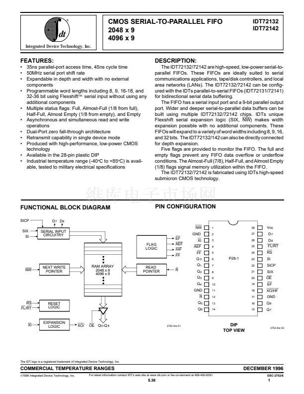
The FIFO has a serial input port and a 9-bit parallel output
port. Wider and deeper serial-to-parallel data buffers can be
built using multiple IDT72132/72142 chips. IDTs unique
Flexshift serial expansion logic (SIX,
) makes width
expansion possible with no additional components. These
FIFOs will expand to a variety of word widths including 8, 9, 16,
and 32 bits. The IDT72132/142 can also be directly connected
for depth expansion.
Five flags are provided to monitor the FIFO. The full and
empty flags prevent any FIFO data overflow or underflow
conditions. The Almost-Full (7/8), Half-Full, and Almost Empty
(1/8) flags signal memory utilization within the FIFO.
The IDT72132/72142 is fabricated using IDTs high-speed
submicron CMOS technology.
NW
FUNCTIONAL BLOCK DIAGRAM
SICP
SIX
SI
D
7
D
8
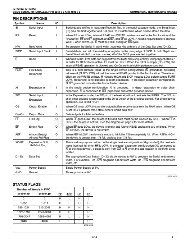
PIN CONFIGURATION
NW
1
2
3
4
5
6
7
8
9
10
11
12
13
14
28
27
26
25
24
Vcc
D
7
D
8
FL/RT
RS
SI
SICP
SIX
OE
EF
XO/HF
GND
Q
8
Q
7
SERIAL INPUT
CIRCUITRY
FLAG
LOGIC
GND
EF
AEF
/HF
FF
XI
AEF
FF
Q
0
Q
1
Q
2
Q
3
Q
4
GND
R
Q
5
Q
6
NW
NEXT WRITE
POINTER
RAM ARRAY
2048 x 9
4096 x 9
READ
POINTER
P28-1
&
C28-3
23
22
21
20
19
18
17
16
15
R
RS
FL/RT
RESET
LOGIC
XI
EXPANSION
LOGIC
XO/
OE Q
0
-Q
8
2752 drw 01
DIP
TOP VIEW
2752 drw 02
The IDT logo is a registered trademark of Integrated Device Technology, Inc.
COMMERCIAL TEMPERATURE RANGES
漏1996
Integrated Device Technology, Inc.
For latest information contact IDT's web site at www.idt.com or fax-on-demand at 408-492-8391.
DECEMBER 1996
DSC-2752/6
5.36
1


 1
1
 2
2
 3
3
 4
4
 5
5
 6
6
 7
7
 8
8
 9
9
 10
10
 11
11
 12
12
 13
13
