IRFP140N
TM
Data Sheet
March 2000
File Number
4841
33A, 100V, 0.040 Ohm, N-Channel Power MOSFET
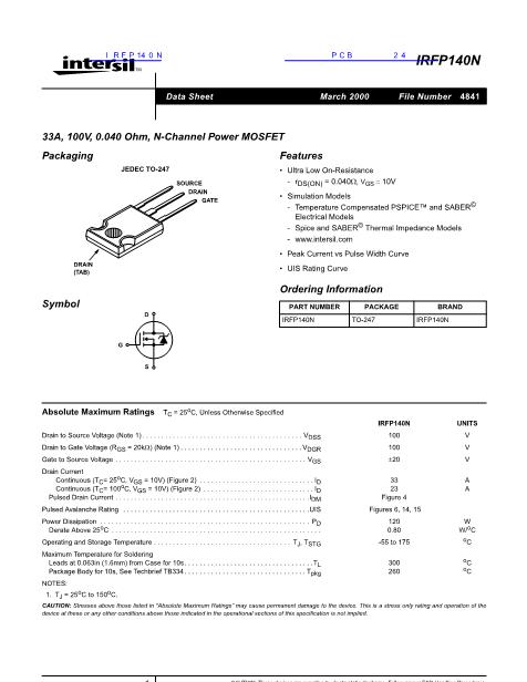
Packaging
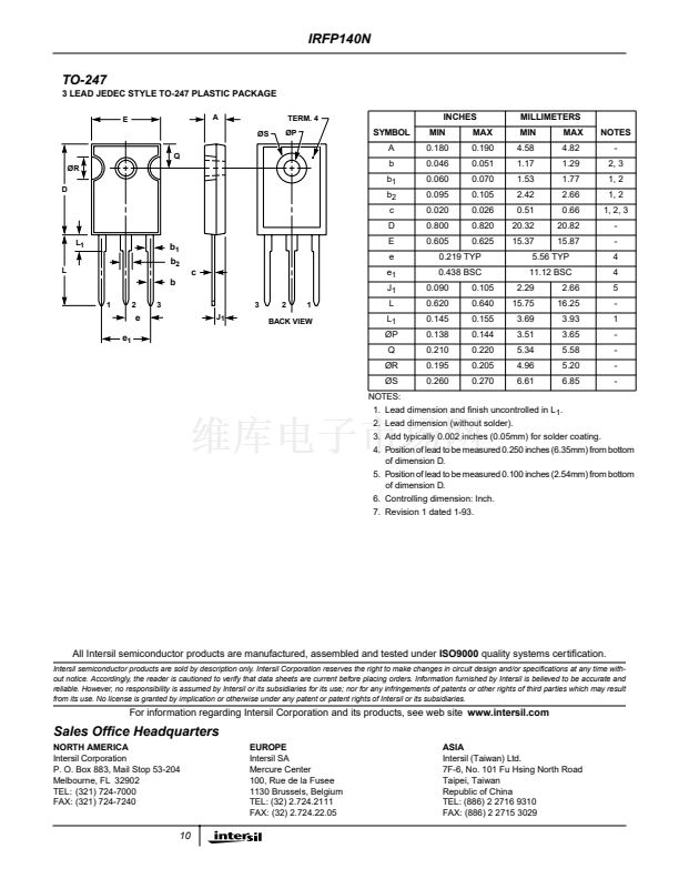
JEDEC TO-247
SOURCE
DRAIN
GATE
Features
鈥?Ultra Low On-Resistance
- r
DS(ON)
= 0.040鈩?
V
GS
=
10V
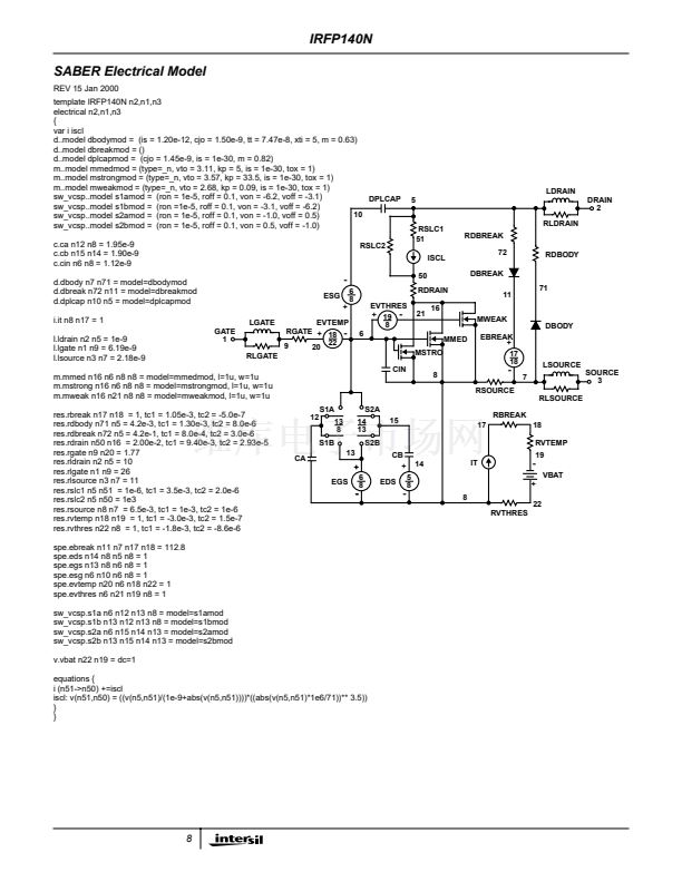
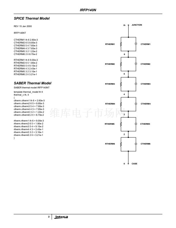
鈥?Simulation Models
- Temperature Compensated PSPICE鈩?and SABER
漏
Electrical Models
- Spice and SABER
漏
Thermal Impedance Models
- www.intersil.com
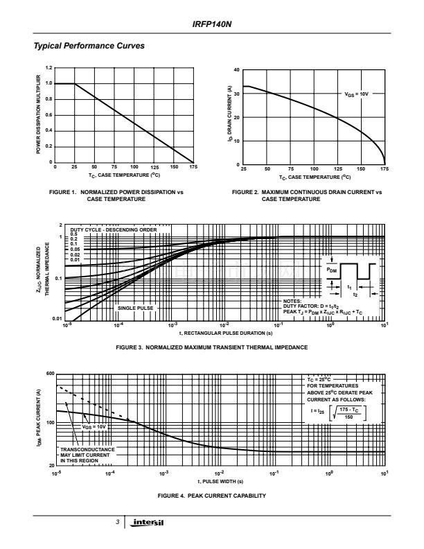
鈥?Peak Current vs Pulse Width Curve
DRAIN
(TAB)
鈥?UIS Rating Curve
Ordering Information
Symbol
D
PART NUMBER
IRFP140N
PACKAGE
TO-247
BRAND
IRFP140N
G
S
Absolute Maximum Ratings
T
C
= 25
o
C, Unless Otherwise Specified
IRFP140N
UNITS
V
V
V
A
A
100
100
卤20
33
23
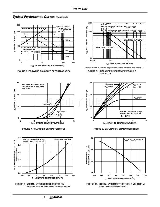
Figure 4
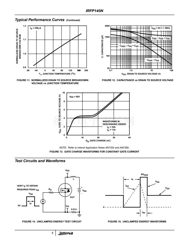
Figures 6, 14, 15
120
0.80
-55 to 175
300
260
W
W/
o
C
o
C
o
C
o
C
Drain to Source Voltage (Note 1) . . . . . . . . . . . . . . . . . . . . . . . . . . . . . . . . . . . . . . . . . . V
DSS
Drain to Gate Voltage (R
GS
= 20k鈩? (Note 1) . . . . . . . . . . . . . . . . . . . . . . . . . . . . . . . . V
DGR
Gate to Source Voltage . . . . . . . . . . . . . . . . . . . . . . . . . . . . . . . . . . . . . . . . . . . . . . . . . . V
GS
Drain Current
Continuous (T
C
= 25
o
C, V
GS
= 10V) (Figure 2) . . . . . . . . . . . . . . . . . . . . . . . . . . . . . . I
D
Continuous (T
C
= 100
o
C, V
GS
= 10V) (Figure 2) . . . . . . . . . . . . . . . . . . . . . . . . . . . . . I
D
Pulsed Drain Current . . . . . . . . . . . . . . . . . . . . . . . . . . . . . . . . . . . . . . . . . . . . . . . . . . .I
DM
Pulsed Avalanche Rating . . . . . . . . . . . . . . . . . . . . . . . . . . . . . . . . . . . . . . . . . . . . . . . . .UIS
Power Dissipation . . . . . . . . . . . . . . . . . . . . . . . . . . . . . . . . . . . . . . . . . . . . . . . . . . . . . . . P
D
Derate Above 25
o
C . . . . . . . . . . . . . . . . . . . . . . . . . . . . . . . . . . . . . . . . . . . . . . . . . . . . . . .
Operating and Storage Temperature . . . . . . . . . . . . . . . . . . . . . . . . . . . . . . . . . . . . T
J
, T
STG
Maximum Temperature for Soldering
Leads at 0.063in (1.6mm) from Case for 10s. . . . . . . . . . . . . . . . . . . . . . . . . . . . . . . . . .T
L
Package Body for 10s, See Techbrief TB334 . . . . . . . . . . . . . . . . . . . . . . . . . . . . . . . . T
pkg
NOTES:
1. T
J
= 25
o
C to 150
o
C.
CAUTION:
Stresses above those listed in 鈥淎bsolute Maximum Ratings鈥?may cause permanent damage to the device. This is a stress only rating and operation of the
device at these or any other conditions above those indicated in the operational sections of this speci铿乧ation is not implied.
1
CAUTION: These devices are sensitive to electrostatic discharge. Follow proper ESD Handling Procedures.
PSPICE庐 is a registered trademark of MicroSim Corporation. SABER漏 is a Copyright of Analogy Inc.
1-888-INTERSIL or 321-724-7143 | Intersil and Design is a trademark of Intersil Corporation.
|
Copyright
漏
Intersil Corporation 2000


 1
1
 2
2
 3
3
 4
4
 5
5
 6
6
 7
7
 8
8
 9
9
 10
10
