鈥?/div>
Input Bus
A2
GLB
Logic
Array
D Q
D Q
A5
D Q
f
max
= 180 MHz Maximum Operating Frequency
t
pd
= 5.0 ns Propagation Delay
TTL Compatible Inputs and Outputs
Electrically Erasable and Reprogrammable
Non-Volatile
100% Tested at Time of Manufacture
Unused Product Term Shutdown Saves Power
N
EW
A3
A4
0139Bisp/2000
鈥?IN-SYSTEM PROGRAMMABLE
鈥?OFFERS THE EASE OF USE AND FAST SYSTEM
SPEED OF PLDs WITH THE DENSITY AND FLEXIBILITY
OF FIELD PROGRAMMABLE GATE ARRAYS
鈥?Complete Programmable Device Can Combine Glue
Logic and Structured Designs
鈥?Enhanced Pin Locking Capability
鈥?Three Dedicated Clock Input Pins
鈥?Synchronous and Asynchronous Clocks
鈥?Programmable Output Slew Rate Control to
Minimize Switching Noise
鈥?Flexible Pin Placement
鈥?Optimized Global Routing Pool Provides Global
Interconnectivity
LS
I2
03
2E
鈥?In-System Programmable (ISP鈩? 5V Only
鈥?Increased Manufacturing Yields, Reduced Time-to-
Market and Improved Product Quality
鈥?Reprogram Soldered Devices for Faster Prototyping
Copyright 漏 2002 Lattice Semiconductor Corp. All brand or product names are trademarks or registered trademarks of their respective holders. The specifications and information herein are subject
to change without notice.
U
SE
is
p
FO
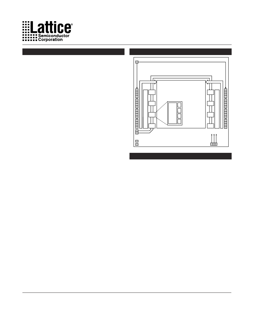
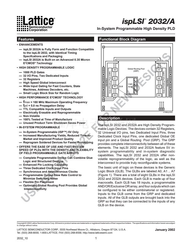
The ispLSI 2032 and 2032A are High Density Program-
mable Logic Devices. The devices contain 32 Registers,
32 Universal I/O pins, two Dedicated Input Pins, three
Dedicated Clock Input Pins, one dedicated Global OE
input pin and a Global Routing Pool (GRP). The GRP
provides complete interconnectivity between all of these
elements. The ispLSI 2032 and 2032A feature 5V in-
system programmability and in-system diagnostic
capabilities. The ispLSI 2032 and 2032A offer non-
volatile reprogrammability of the logic, as well as the
interconnect to provide truly reconfigurable systems.
The basic unit of logic on these devices is the Generic
Logic Block (GLB). The GLBs are labeled A0, A1 .. A7
(Figure 1). There are a total of eight GLBs in the ispLSI
2032 and 2032A devices. Each GLB is made up of four
macrocells. Each GLB has 18 inputs, a programmable
AND/OR/Exclusive OR array, and four outputs which can
be configured to be either combinatorial or registered.
Inputs to the GLB come from the GRP and dedicated
inputs. All of the GLB outputs are brought back into the
GRP so that they can be connected to the inputs of any
GLB on the device.
R
Description
LATTICE SEMICONDUCTOR CORP., 5555 Northeast Moore Ct., Hillsboro, Oregon 97124, U.S.A.
Tel. (503) 268-8000; 1-800-LATTICE; FAX (503) 268-8556; http://www.latticesemi.com
January 2002
2032_10
1
Input Bus
A1
A6
Output Routing Pool (ORP)
Global Routing Pool
(GRP)
N
S
A7


 1
1
 2
2
 3
3
 4
4
 5
5
 6
6
 7
7
 8
8
 9
9
 10
10
 11
11
 12
12
 13
13
 14
14
 15
15
