鈥?/div>
Pb鈭扚ree Packages are Available*
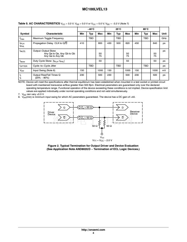
500 ps Typical Propagation Delays
50 ps Output鈭扥utput Skews
ESD Protection: >2 kV Human Body Model
The 100 Series Contains Temperature Compensation
PECL Mode Operating Range: V
CC
= 3.0 V to 3.8 V
with V
EE
= 0 V
NECL Mode Operating Range: V
CC
= 0 V
with V
EE
=
鈭?.0
V to
鈭?.8
V
Internal Input Pulldown Resistors
Q Output will Default LOW with Inputs Open or at V
EE
Meets or Exceeds JEDEC Spec EIA/JESD78 IC Latchup Test
Moisture Sensitivity Level 1
For Additional Information, see Application Note AND8003/D
Flammability Rating: UL 94 V鈭? @ 0.125 in,
Oxygen Index: 28 to 34
Transistor Count = 143 devices
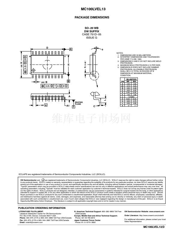
SO鈭?0 WB
DW SUFFIX
CASE 751D
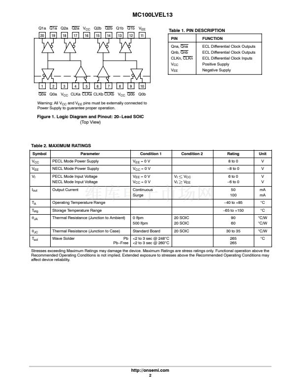
MARKING DIAGRAM*
20
100LVEL13
AWLYYWWG
1
A
WL
YY
WW
G
= Assembly Location
= Wafer Lot
= Year
= Work Week
= Pb鈭扚ree Package
*For additional marking information, refer to
Application Note AND8002/D.
ORDERING INFORMATION
See detailed ordering and shipping information in the package
dimensions section on page 5 of this data sheet.
*For additional information on our Pb鈭扚ree strategy and soldering details, please
download the ON Semiconductor Soldering and Mounting Techniques
Reference Manual, SOLDERRM/D.
漏
Semiconductor Components Industries, LLC, 2006
November, 2006
鈭?/div>
Rev. 5
1
Publication Order Number:
MC100LVEL13/D


 1
1
 2
2
 3
3
 4
4
 5
5
 6
6
