鈥?/div>
325 ps Propagation Delay
High Bandwidth Output Transitions
The 100 Series Contains Temperature Compensation
PECL Mode Operating Range: V
CC
= 3.0 V to 3.8 V
with V
EE
= 0 V
NECL Mode Operating Range: V
CC
= 0 V
with V
EE
=
鈭?.0
V to
鈭?.8
V
Internal Input Pulldown Resistors D Inputs;
Pullup and Pulldown on D Inputs
Q Output will Default LOW with Inputs Open or at V
EE
Pb鈭扚ree Packages are Available*
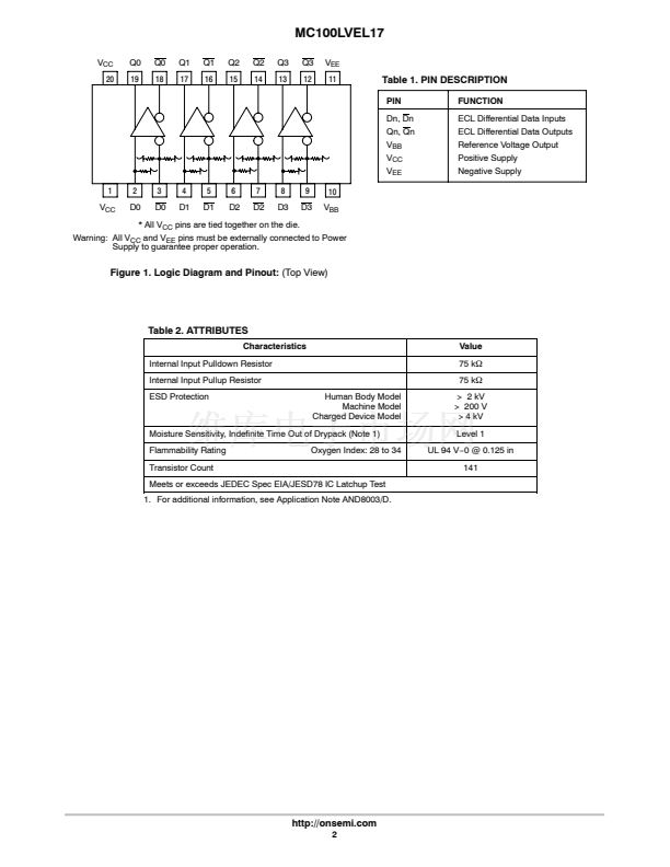
MARKING DIAGRAM*
20
100LVEL17
AWLYYWWG
1
A
WL
YY
WW
G
= Assembly Location
= Wafer Lot
= Year
= Work Week
= Pb鈭扚ree Package
*For additional marking information, refer to
Application Note AND8002/D.
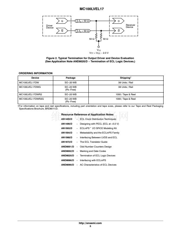
ORDERING INFORMATION
See detailed ordering and shipping information in the package
dimensions section on page 5 of this data sheet.
*For additional information on our Pb鈭扚ree strategy and soldering details, please
download the ON Semiconductor Soldering and Mounting Techniques
Reference Manual, SOLDERRM/D.
漏
Semiconductor Components Industries, LLC, 2006
November, 2006
鈭?/div>
Rev. 7
1
Publication Order Number:
MC100LVEL17/D


 1
1
 2
2
 3
3
 4
4
 5
5
 6
6
