MC100LVEL34
3.3V ECL
梅
2,
梅
4,
梅
8 Clock
Generation Chip
Description
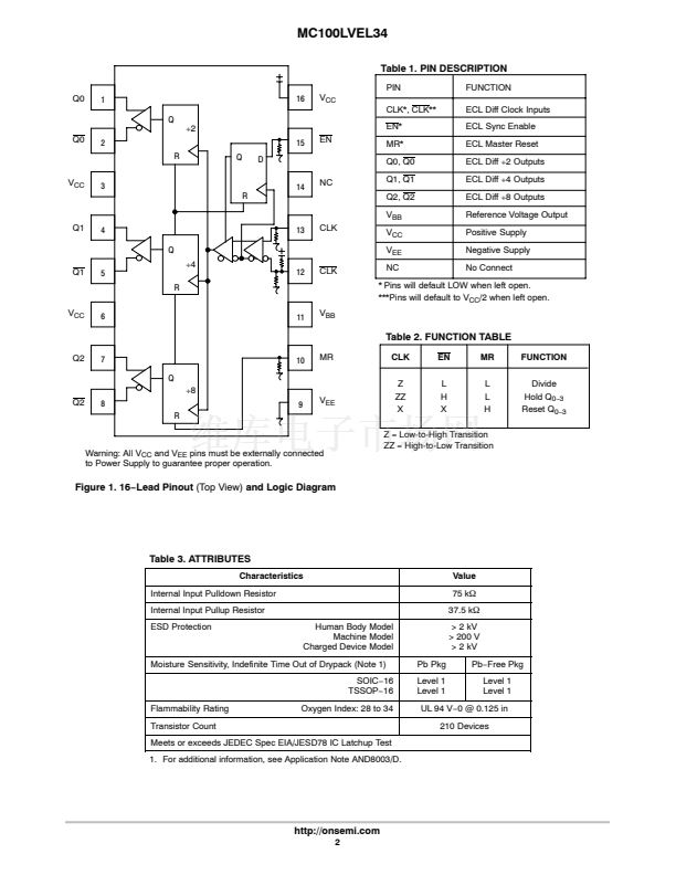
The MC100LVEL34 is a low skew
梅
2,
梅
4,
梅
8 clock generation
chip designed explicitly for low skew clock generation applications.
The internal dividers are synchronous to each other, therefore, the
common output edges are all precisely aligned. The V
BB
pin, an
internally generated voltage supply, is available to this device only.
For single鈭抏nded input conditions, the unused differential input is
connected to V
BB
as a switching reference voltage. V
BB
may also
rebias AC coupled inputs. When used, decouple V
BB
and V
CC
via a
0.01
mF
capacitor and limit current sourcing or sinking to 0.5 mA.
When not used, V
BB
should be left open.
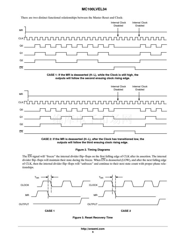
The common enable (EN) is synchronous so that the internal
dividers will only be enabled/disabled when the internal clock is
already in the LOW state. This avoids any chance of generating a runt
clock pulse on the internal clock when the device is enabled/disabled
as can happen with an asynchronous control. An internal runt pulse
could lead to losing synchronization between the internal divider
stages. The internal enable flip-flop is clocked on the falling edge of
the input clock; therefore, all associated specification limits are
referenced to the negative edge of the clock input.
Upon start鈭抲p, the internal flip-flops will attain a random state; the
master reset (MR) input allows for the synchronization of the internal
dividers, as well as multiple LVEL34s in a system.
Features
http://onsemi.com
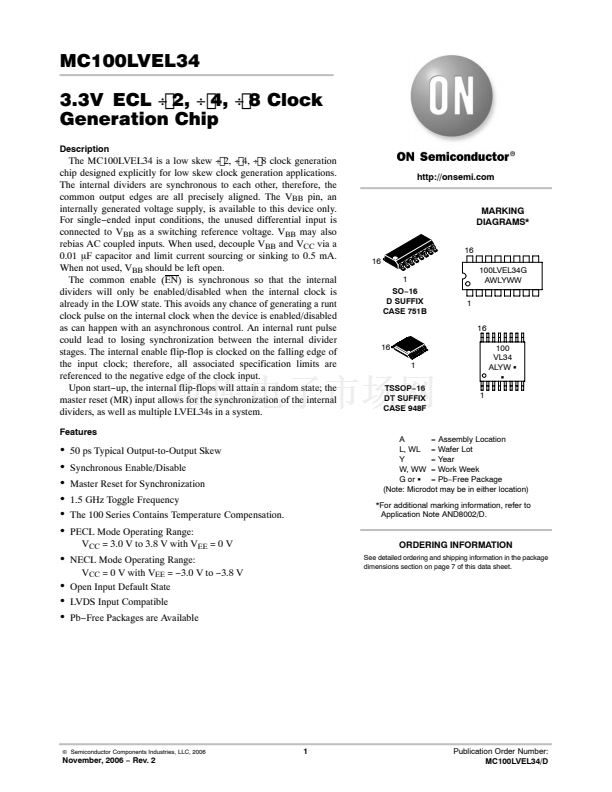
MARKING
DIAGRAMS*
16
16
1
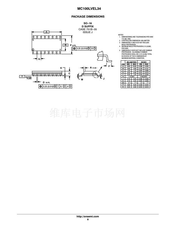
SO鈭?6
D SUFFIX
CASE 751B
1
16
16
1
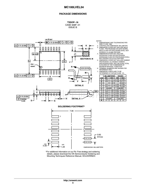
TSSOP鈭?6
DT SUFFIX
CASE 948F
100
VL34
ALYW
G
G
1
100LVEL34G
AWLYWW
鈥?/div>
鈥?/div>
鈥?/div>
鈥?/div>
鈥?/div>
鈥?/div>
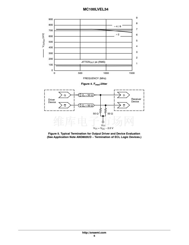
50 ps Typical Output-to-Output Skew
Synchronous Enable/Disable
Master Reset for Synchronization
1.5 GHz Toggle Frequency
The 100 Series Contains Temperature Compensation.
PECL Mode Operating Range:
V
CC
= 3.0 V to 3.8 V with V
EE
= 0 V
A
= Assembly Location
L, WL = Wafer Lot
Y
= Year
W, WW = Work Week
G or
G
= Pb鈭扚ree Package
(Note: Microdot may be in either location)
*For additional marking information, refer to
Application Note AND8002/D.
ORDERING INFORMATION
See detailed ordering and shipping information in the package
dimensions section on page 7 of this data sheet.
鈥?/div>
NECL Mode Operating Range:
V
CC
= 0 V with V
EE
=
鈭?.0
V to
鈭?.8
V
鈥?/div>
Open Input Default State
鈥?/div>
LVDS Input Compatible
鈥?/div>
Pb鈭扚ree Packages are Available
漏
Semiconductor Components Industries, LLC, 2006
November, 2006
鈭?/div>
Rev. 2
1
Publication Order Number:
MC100LVEL34/D
MC100LVEL34_06 PDF文件相关型号
MC100LVEL34DR2G
MC100LVEL34_06相关型号PDF文件下载


 1
1
 2
2
 3
3
 4
4
 5
5
 6
6
 7
7
 8
8
 9
9
 10
10
