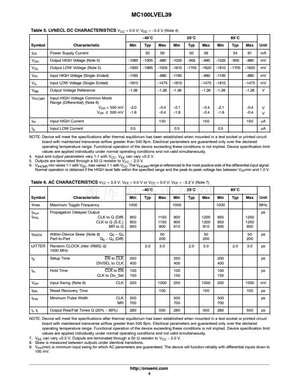
MC100LVEL39
3.3V ECL
梅2/4, 梅4/6
Clock
Generation Chip
Description
The MC100LVEL39 is a low skew
梅2/4, 梅4/6
clock generation chip
designed explicitly for low skew clock generation applications. The
internal dividers are synchronous to each other, therefore, the common
output edges are all precisely aligned. The device can be driven by
either a differential or single-ended input signal. In addition, by using
the V
BB
output, a sinusoidal source can be AC coupled into the device.
The common enable (EN) is synchronous so that the internal dividers
will only be enabled/disabled when the internal clock is already in the
LOW state. This avoids any chance of generating a runt clock pulse on
the internal clock when the device is enabled/disabled as can happen with
an asynchronous control. An internal runt pulse could lead to losing
synchronization between the internal divider stages. The internal enable
flip鈭抐lop is clocked on the falling edge of the input clock, therefore, all
associated specification limits are referenced to the negative edge of the
clock input.
Upon startup, the internal flip-flops will attain a random state;
therefore, for systems which utilize multiple LVEL39s, the Master Reset
(MR) input must be asserted to ensure synchronization. For systems
which only use one LVEL39, the MR pin need not be exercised as the
internal divider design ensures synchronization between the
梅2/4
and the
梅4/6
outputs of a single device.
The V
BB
pin, an internally generated voltage supply, is available to this
device only. For single-ended input conditions, the unused differential
input is connected to V
BB
as a switching reference voltage. V
BB
may also
rebias AC coupled inputs. When used, decouple V
BB
and V
CC
via a
0.01
mF
capacitor and limit current sourcing or sinking to 0.5 mA. When
not used, V
BB
should be left open.
Features
http://onsemi.com
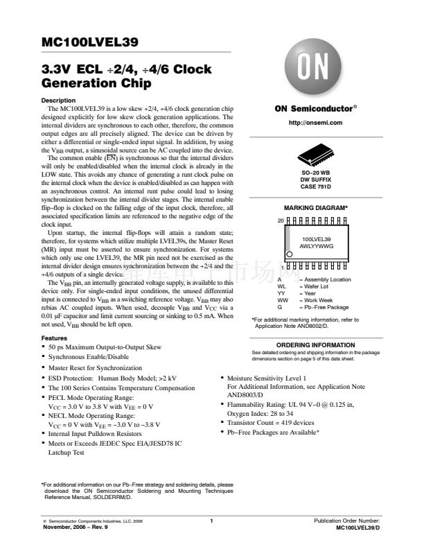
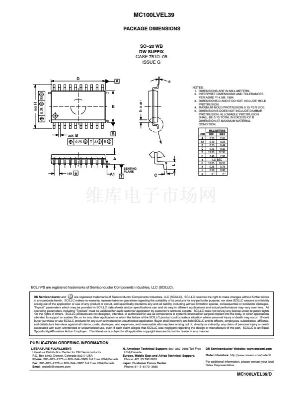
SO鈭?0 WB
DW SUFFIX
CASE 751D
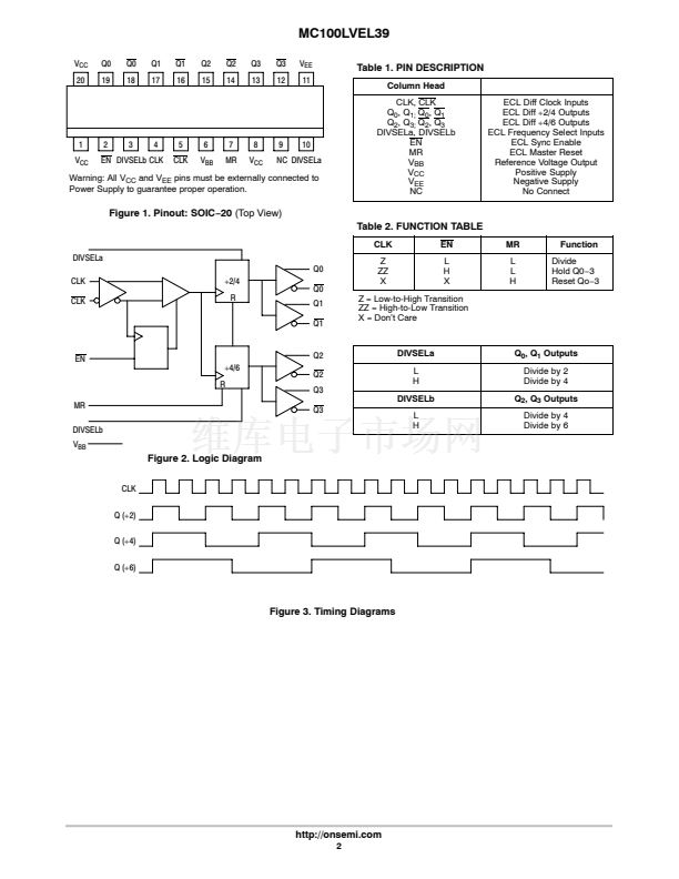
MARKING DIAGRAM*
20
100LVEL39
AWLYYWWG
1
A
WL
YY
WW
G
= Assembly Location
= Wafer Lot
= Year
= Work Week
= Pb鈭扚ree Package
*For additional marking information, refer to
Application Note AND8002/D.
鈥?/div>
鈥?/div>
鈥?/div>
鈥?/div>
鈥?/div>
鈥?/div>
50 ps Maximum Output-to-Output Skew
Synchronous Enable/Disable
Master Reset for Synchronization
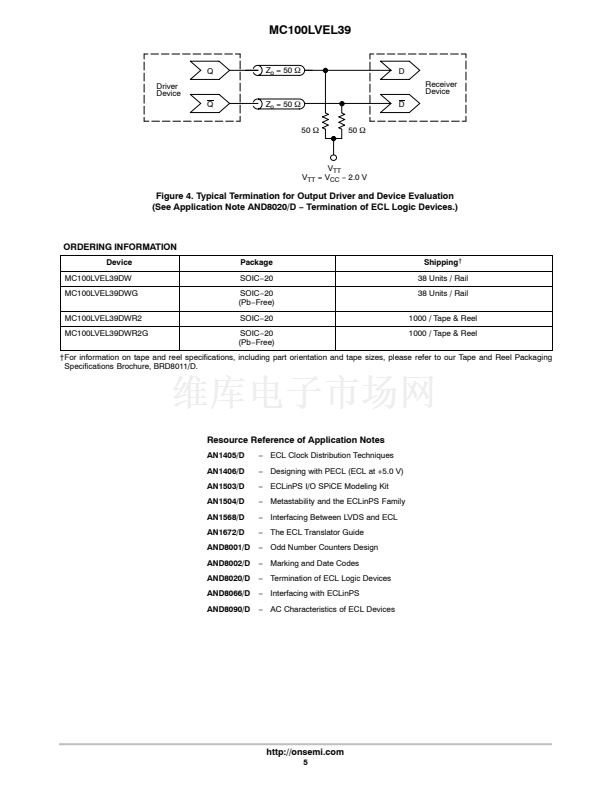
ORDERING INFORMATION
See detailed ordering and shipping information in the package
dimensions section on page 5 of this data sheet.
ESD Protection: Human Body Model; >2 kV
The 100 Series Contains Temperature Compensation
PECL Mode Operating Range:
V
CC
= 3.0 V to 3.8 V with V
EE
= 0 V
鈥?/div>
NECL Mode Operating Range:
V
CC
= 0 V with V
EE
=
鈭?.0
V to
鈭?.8
V
鈥?/div>
Internal Input Pulldown Resistors
鈥?/div>
Meets or Exceeds JEDEC Spec EIA/JESD78 IC
Latchup Test
鈥?/div>
Moisture Sensitivity Level 1
For Additional Information, see Application Note
AND8003/D
鈥?/div>
Flammability Rating: UL 94 V鈭? @ 0.125 in,
Oxygen Index: 28 to 34
鈥?/div>
Transistor Count = 419 devices
鈥?/div>
Pb鈭扚ree Packages are Available*
*For additional information on our Pb鈭扚ree strategy and soldering details, please
download the ON Semiconductor Soldering and Mounting Techniques
Reference Manual, SOLDERRM/D.
漏
Semiconductor Components Industries, LLC, 2006
November, 2006
鈭?/div>
Rev. 9
1
Publication Order Number:
MC100LVEL39/D
MC100LVEL39DWG PDF文件相关型号
MC100LVEL39DWR2,MC100LVEL39DWR2G
MC100LVEL39DWG 产品属性
38
集成电路 (IC)
时钟/计时 - 时钟发生器,PLL,频率合成器
100LVEL
时钟发生器
无
LVDS,NECL,PECL
ECL
1
1:4
是/是
1GHz
是/无
±3 V ~ 3.8 V
-40°C ~ 85°C
表面贴装
20-SOIC(0.295",7.50mm 宽)
20-SOIC
管件
MC100LVEL39DWGOS
MC100LVEL39DWG相关型号PDF文件下载


 1
1
 2
2
 3
3
 4
4
 5
5
 6
6
