鈥?/div>
Pb鈭扚ree Packages are Available*
4
5
9
10
12
13
V
BB
*
V
CC1
= Pin 1
V
CC2
= Pin 16
V
EE
= Pin 8
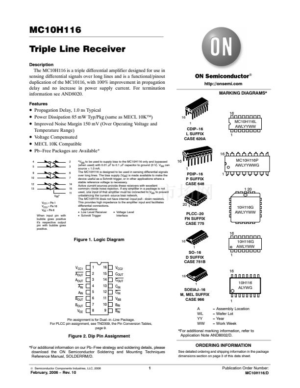
When input pin with
bubble goes positive
it鈥檚 respective output
pin with bubble goes
positive.
2
3
6
7
14
15
11
16
1
16
MC10H116L
AWLYYWW
1
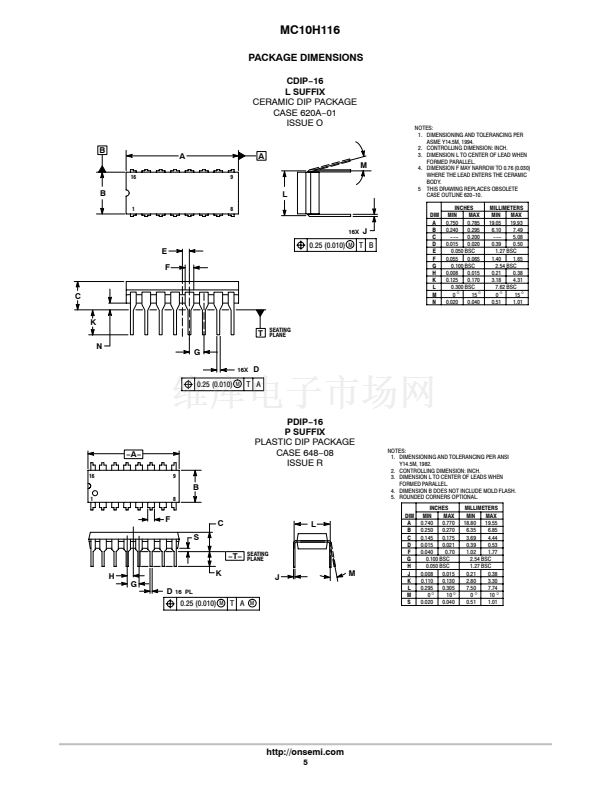
CDIP鈭?6
L SUFFIX
CASE 620A
16
16
1
PDIP鈭?6
P SUFFIX
CASE 648
1
MC10H116P
AWLYYWWG
*V
BB
to be used to supply bias to the MC10H116 only and bypassed
(when used) with 0.01
mF
to 0.1
mF
capacitor to ground (0 V). V
BB
can
source < 1.0 mA.
The MC10H116 is designed to be used in sensing differential signals
over long lines. The bias supply (V
BB
) is made available to make the
device useful as a Schmitt trigger, or in other applications where a
stable reference voltage is necessary.
Active current sources provide these receivers with excellent
common鈭抦ode noise rejection. If any amplifier in a package is not
used, one input of that amplifier must be connected to V
BB
to prevent
unbalancing the current鈭抯ource bias network.
The MC10H116 does not have internal鈭抜nput pull鈭?down resistors.
This provides high impedance to the amplifier input and facilitates
differential connections.
Applications:
鈥?/div>
Low Level Receiver
鈥?/div>
Voltage Level
鈥?/div>
Schmitt Trigger
Interface
1 20
20 1
PLCC鈭?0
FN SUFFIX
CASE 775
16
10H116G
AWLYYWW
Figure 1. Logic Diagram
16
1
10H116G
AWLYWW
1
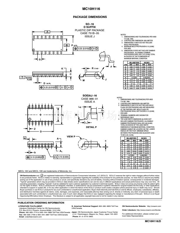
SO鈭?6
D SUFFIX
CASE 751B
V
CC1
A
OUT
A
OUT
A
IN
A
IN
B
OUT
B
OUT
V
EE
1
2
3
4
5
6
7
8
16
15
14
13
12
11
10
9
V
CC2
C
OUT
C
OUT
C
IN
C
IN
V
BB
B
IN
B
IN
16
1
16
10H116
ALYWG
1
= Assembly Location
= Wafer Lot
= Year
= Work Week
SOEIAJ鈭?6
M, MEL SUFFIX
CASE 966
A
WL
YY
WW
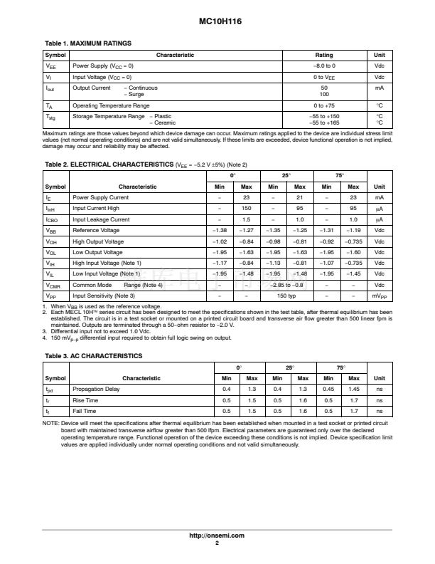
Pin assignment is for Dual鈭抜n鈭扡ine Package.
For PLCC pin assignment, see TND309, the Pin Conversion Tables,
page 9.
Figure 2. Dip Pin Assignment
*For additional information on our Pb鈭扚ree strategy and soldering details, please
download the ON Semiconductor Soldering and Mounting Techniques
Reference Manual, SOLDERRM/D.
漏
Semiconductor Components Industries, LLC, 2006
*For additional marking information, refer to
Application Note AND8002/D.
ORDERING INFORMATION
See detailed ordering and shipping information in the package
dimensions section on page 3 of this data sheet.
February, 2006
鈭?/div>
Rev. 10
1
Publication Order Number:
MC10H116/D


 1
1
 2
2
 3
3
 4
4
 5
5
 6
6
