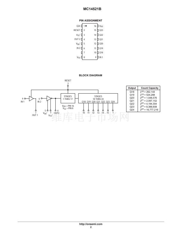
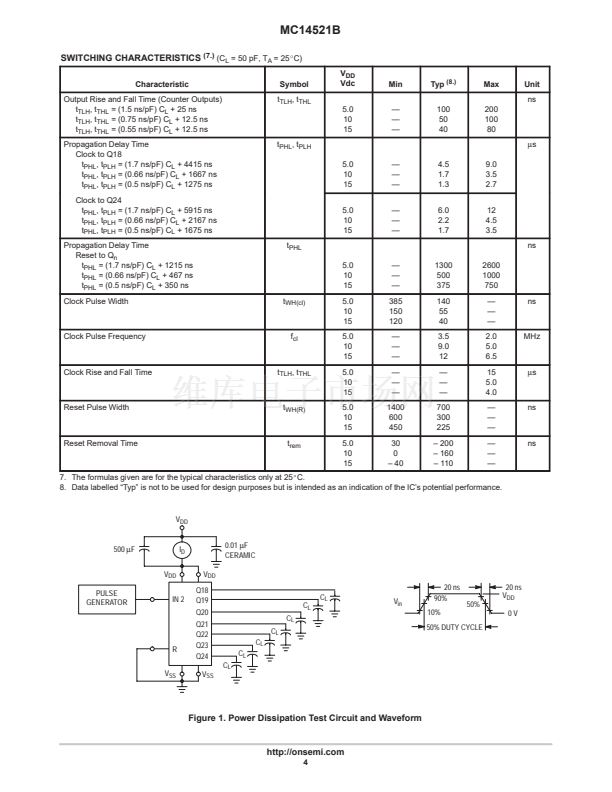
鈥?/div>
Pins Brought Out on Crystal Oscillator Inverter to
Allow the Connection of External Resistors for Low鈥揚ower
Operation
Supply Voltage Range = 3.0 Vdc to 18 Vdc
Capable of Driving Two Low鈥損ower TTL Loads or One Low鈥損ower
Schottky TTL Load over the Rated Temperature Range.
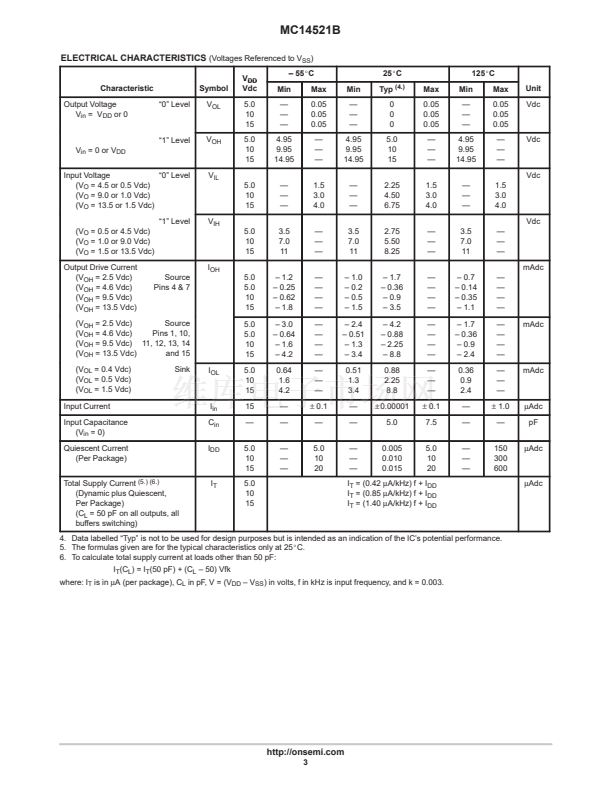
MAXIMUM RATINGS
(Voltages Referenced to V
SS
) (Note 2.)
Symbol
V
DD
V
in
, V
out
I
in
, I
out
P
D
T
A
T
stg
T
L
Parameter
DC Supply Voltage Range
Input or Output Voltage Range
(DC or Transient)
Input or Output Current
(DC or Transient) per Pin
Power Dissipation,
per Package (Note 3.)
Ambient Temperature Range
Storage Temperature Range
Lead Temperature
(8鈥揝econd Soldering)
Value
鈥?0.5 to +18.0
鈥?0.5 to V
DD
+ 0.5
卤
10
500
鈥?55 to +125
鈥?65 to +150
260
Unit
V
V
mA
mW
掳C
掳C
掳C
A
= Assembly Location
WL or L = Wafer Lot
YY or Y = Year
WW or W = Work Week
ORDERING INFORMATION
Device
MC14521BCP
MC14521BD
MC14521BDR2
MC14521BF
MC14521BFEL
MC14521BFR2
Package
PDIP鈥?6
SOIC鈥?6
SOIC鈥?6
SOEIAJ鈥?6
SOEIAJ鈥?6
SOEIAJ鈥?6
Shipping
2000/Box
48/Rail
2500/Tape & Reel
See Note 1.
See Note 1.
See Note 1.
2. Maximum Ratings are those values beyond which damage to the device
may occur.
3. Temperature Derating:
Plastic 鈥淧 and D/DW鈥?Packages: 鈥?7.0 mW/
_
C From 65
_
C To 125
_
C
This device contains protection circuitry to guard against damage due to high
static voltages or electric fields. However, precautions must be taken to avoid
applications of any voltage higher than maximum rated voltages to this
high鈥搃mpedance circuit. For proper operation, V
in
and V
out
should be constrained
(V
in
or V
out
)
V
DD
.
to the range V
SS
Unused inputs must always be tied to an appropriate logic voltage level (e.g.,
either V
SS
or V
DD
). Unused outputs must be left open.
1. For ordering information on the EIAJ version of
the SOIC packages, please contact your local
ON Semiconductor representative.
v
v
漏
Semiconductor Components Industries, LLC, 2000
1
March, 2000 鈥?Rev. 3
Publication Order Number:
MC14521B/D


 1
1
 2
2
 3
3
 4
4
 5
5
 6
6
 7
7
 8
8
 9
9
 10
10
 11
11
 12
12
