鈥?/div>
In Tape and Reel. R1 Suffix = 500 Units per 44 mm, 13 inch Reel.
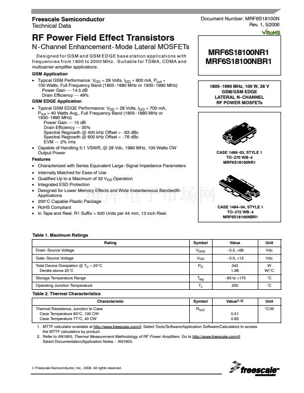
MRF6S18100NR1
MRF6S18100NBR1
1805- 1990 MHz, 100 W, 28 V
GSM/GSM EDGE
LATERAL N - CHANNEL
RF POWER MOSFETs
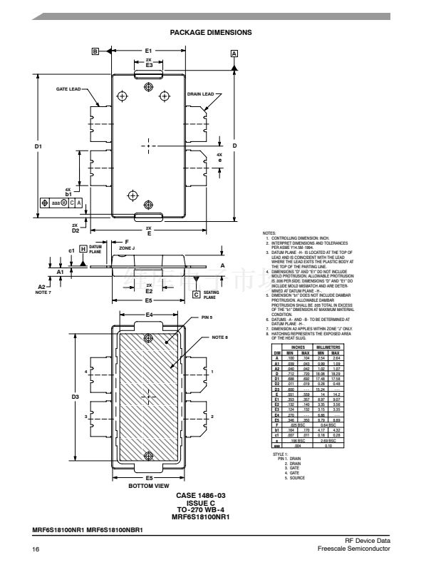
CASE 1486 - 03, STYLE 1
TO - 270 WB - 4
MRF6S18100NR1
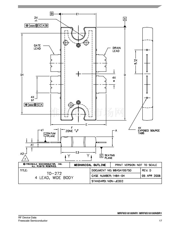
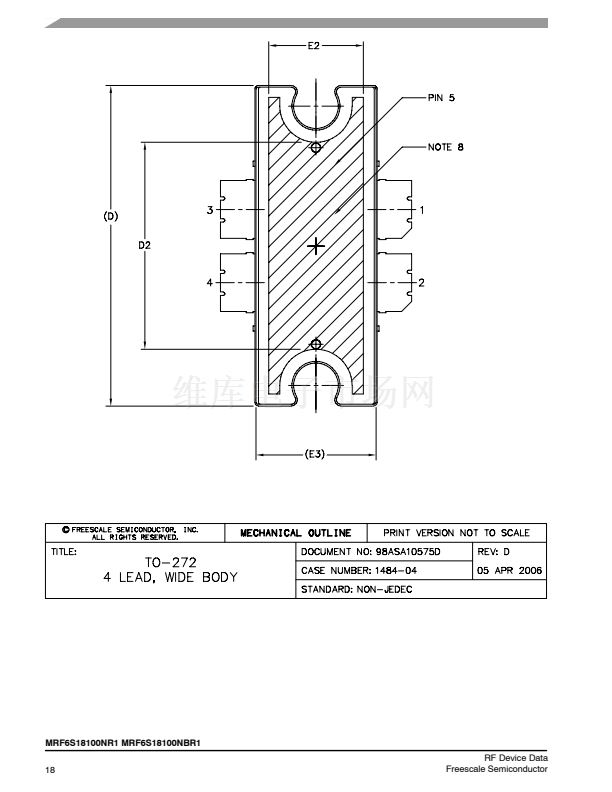
CASE 1484 - 04, STYLE 1
TO - 272 WB - 4
MRF6S18100NBR1
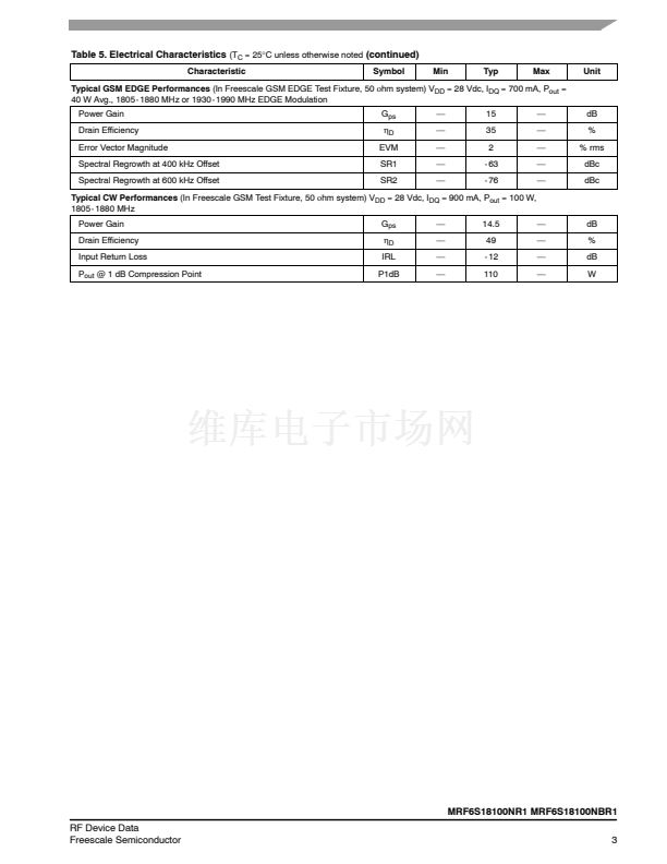
Table 1. Maximum Ratings
Rating
Drain- Source Voltage
Gate- Source Voltage
Total Device Dissipation @ T
C
= 25掳C
Derate above 25掳C
Storage Temperature Range
Operating Junction Temperature
Symbol
V
DSS
V
GS
P
D
T
stg
T
J
Value
- 0.5, +68
- 0.5, +12
343
1.96
- 65 to +175
200
Unit
Vdc
Vdc
W
W/掳C
掳C
掳C
Table 2. Thermal Characteristics
Characteristic
Thermal Resistance, Junction to Case
Case Temperature 80掳C, 100 CW
Case Temperature 77掳C, 40 CW
Symbol
R
胃JC
Value
(1,2)
0.51
0.62
Unit
掳C/W
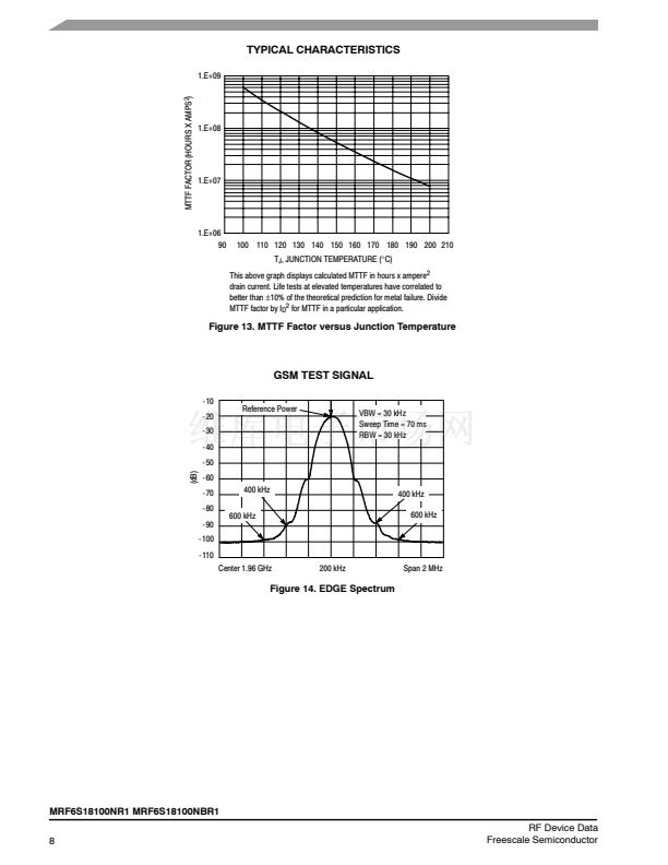
1. MTTF calculator available at http://www.freescale.com/rf. Select Tools/Software/Application Software/Calculators to access
the MTTF calculators by product.
2. Refer to AN1955,
Thermal Measurement Methodology of RF Power Amplifiers.
Go to http://www.freescale.com/rf.
Select Documentation/Application Notes - AN1955.
漏
Freescale Semiconductor, Inc., 2006. All rights reserved.
MRF6S18100NR1 MRF6S18100NBR1
1
RF Device Data
Freescale Semiconductor


 1
1
 2
2
 3
3
 4
4
 5
5
 6
6
 7
7
 8
8
 9
9
 10
10
 11
11
 12
12
 13
13
 14
14
 15
15
 16
16
 17
17
 18
18
 19
19
 20
20
