鈥?/div>
PIC12C671
PIC12C672
PIC12CE673
PIC12CE674
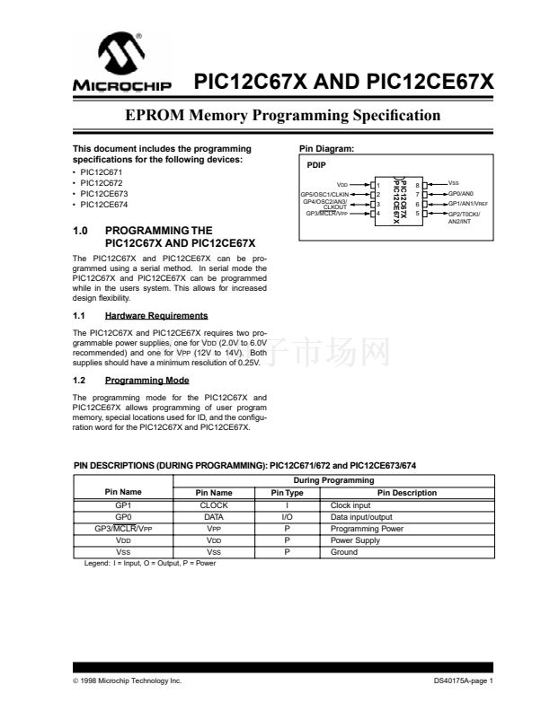
Pin Diagram:
PDIP
PIC12C67X
PIC12CE67X
V
DD
GP5/OSC1/CLKIN
GP4/OSC2/AN3/
CLKOUT
GP3/MCLR/V
PP
1
2
3
4
8
7
6
5
V
SS
GP0/AN0
GP1/AN1/V
REF
GP2/T0CKI/
AN2/INT
1.0
PROGRAMMING THE
PIC12C67X AND PIC12CE67X
The PIC12C67X and PIC12CE67X can be pro-
grammed using a serial method. In serial mode the
PIC12C67X and PIC12CE67X can be programmed
while in the users system. This allows for increased
design 铿俥xibility.
1.1
Hardware Requirements
The PIC12C67X and PIC12CE67X requires two pro-
grammable power supplies, one for V
DD
(2.0V to 6.0V
recommended) and one for V
PP
(12V to 14V). Both
supplies should have a minimum resolution of 0.25V.
1.2
Programming Mode
The programming mode for the PIC12C67X and
PIC12CE67X allows programming of user program
memory, special locations used for ID, and the con铿乬u-
ration word for the PIC12C67X and PIC12CE67X.
PIN DESCRIPTIONS (DURING PROGRAMMING): PIC12C671/672 and PIC12CE673/674
During Programming
Pin Name
GP1
GP0
GP3/MCLR/V
PP
V
DD
V
SS
Pin Name
CLOCK
DATA
V
PP
V
DD
V
SS
Pin Type
I
I/O
P
P
P
Pin Description
Clock input
Data input/output
Programming Power
Power Supply
Ground
Legend: I = Input, O = Output, P = Power
漏
1998 Microchip Technology Inc.
DS40175A-page 1


 1
1
 2
2
 3
3
 4
4
 5
5
 6
6
 7
7
 8
8
 9
9
 10
10
 11
11
 12
12
 13
13
 14
14
