PIC17CXX
EPROM Memory Programming Speci铿乧ation
This document includes the programming
speci铿乧ations for the following devices:
鈥?PIC17C42
鈥?PIC17C42A
鈥?PIC17CR42
鈥?PIC17C43
鈥?PIC17CR43
鈥?PIC17C44
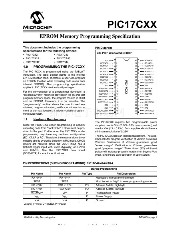
Pin Diagram
40L PDIP, Windowed CERDIP
V
DD
RC0/AD0
RC1/AD1
RC2/AD2
RC3/AD3
RC4/AD4
RC5/AD5
RC6/AD6
RC7/AD7
V
SS
RB0/CAP1
RB1/CAP2
RB2/PWM1
RB3/PWM2
RB4/TCLK12
RB5/TCLK3
RB6
RB7
OSC1/CLKIN
OSC2/CLKOUT
1
2
3
4
5
6
7
8
9
10
11
12
13
14
15
16
17
18
19
20
40
39
38
37
36
35
34
33
32
31
30
29
28
27
26
25
24
23
22
21
RD0/AD8
RD1/AD9
RD2/AD10
RD3/AD11
RD4/AD12
RD5/AD13
RD6/AD14
RD7/AD15
MCLR/V
PP
V
SS
RE0/ALE
RE1/OE
RE2/WR
TEST
RA0/INT
RA1/T0CKI
RA2
RA3
RA4/RX/DT
RA5/TX/CK
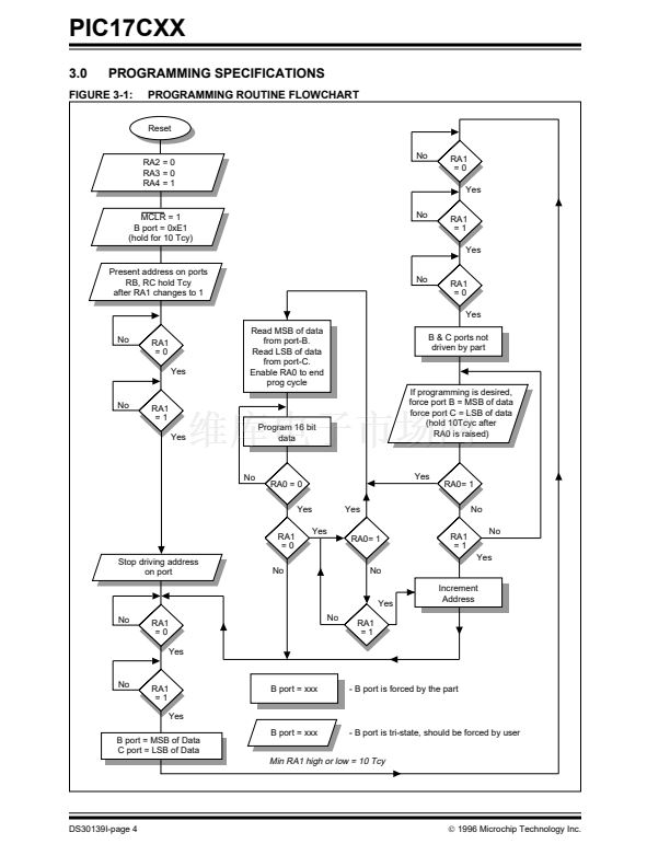
1.0
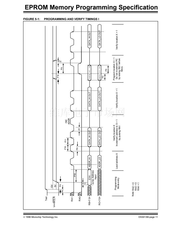
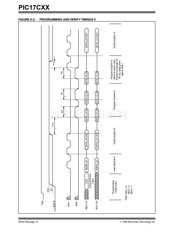
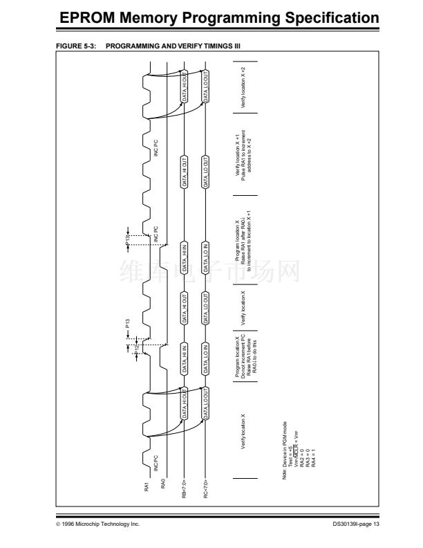
PROGRAMMING THE PIC17CXX
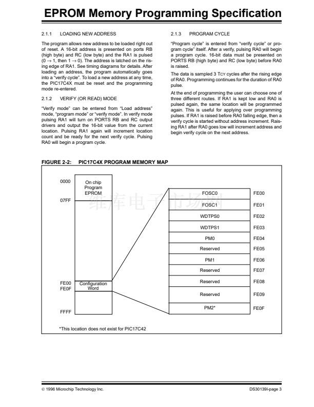
The PIC17CXX is programmed using the TABLWT
instruction. The table pointer points to the internal
EPROM location start. Therefore, a user can program
an EPROM location while executing code (even from
internal EPROM). This programming speci铿乧ation
applies to PIC17CXX devices in all packages.
For the convenience of a programmer developer, a
鈥減rogram & verify鈥?routine is provided in the on-chip test
program memory space, the program resides in ROM
and not EPROM. Therefore, it is not erasable. The
鈥減rogram/verify鈥?routine allows the user to load any
address, program a location, verify a location or incre-
ment to the next location. It allows variable program-
ming pulse width.
PIC17CXX
1.1
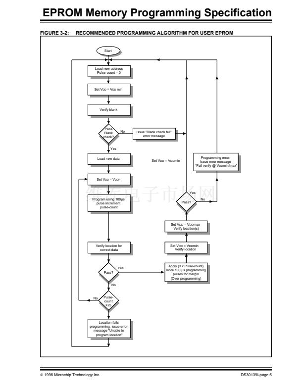
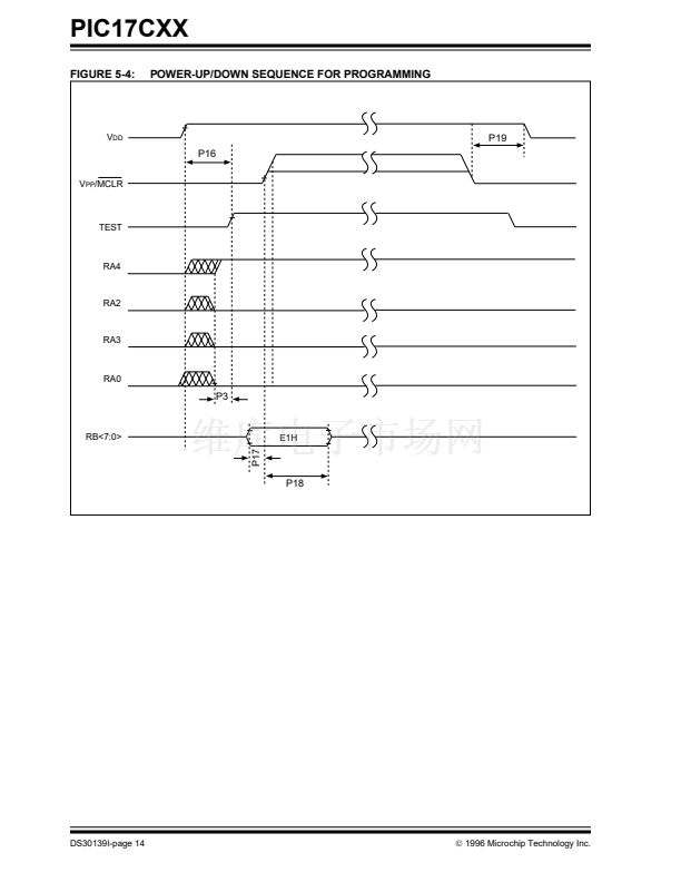
Hardware Requirements
The PIC17CXX requires two programmable power
supplies, one for V
DD
(2.5V to 6.0V recommended) and
one for V
PP
(13
卤
0.25V). Both supplies should have a
minimum resolution of 0.25V.
The PIC17CXX uses an intelligent algorithm. The algo-
rithm calls for program veri铿乧ation at V
DD
min as well as
V
DD
max. Veri铿乧ation at V
DD
min guarantees good
鈥渆rase margin鈥? Veri铿乧ation at V
DD
max guarantees
good 鈥減rogram margin鈥? Three times (3X) additional
pulses will increase program margin then beyond V
DD
(max.) and insure safe operation in user system.
Since the PIC17CXX under programming is actually
executing code from 鈥渂oot ROM,鈥?a clock must be pro-
vided to the part. Furthermore, the PIC17CXX under
programming may have any oscillator con铿乬uration
(EC, XT, LF or RC). Therefore, the external clock driver
must be able to overdrive pulldown in RC mode. CMOS
drivers are required since the OSC1 input has a
Schmitt trigger input with levels (typically) of 0.2V
DD
and 0.8V
DD
. See the PIC17C4X data sheet
(DS30412A) for exact speci铿乧ations.
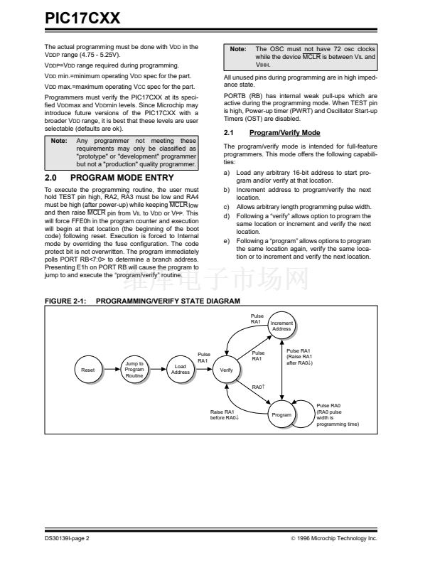
PIN DESCRIPTIONS (DURING PROGRAMMING): PIC17C42/42A/43/44
During Programming
Pin Name
RA <0:4>
TEST
RB <7:0>
RC <7:0>
MCLR/V
PP
V
DD
V
SS
Pin Name
RA <0:4>
TEST
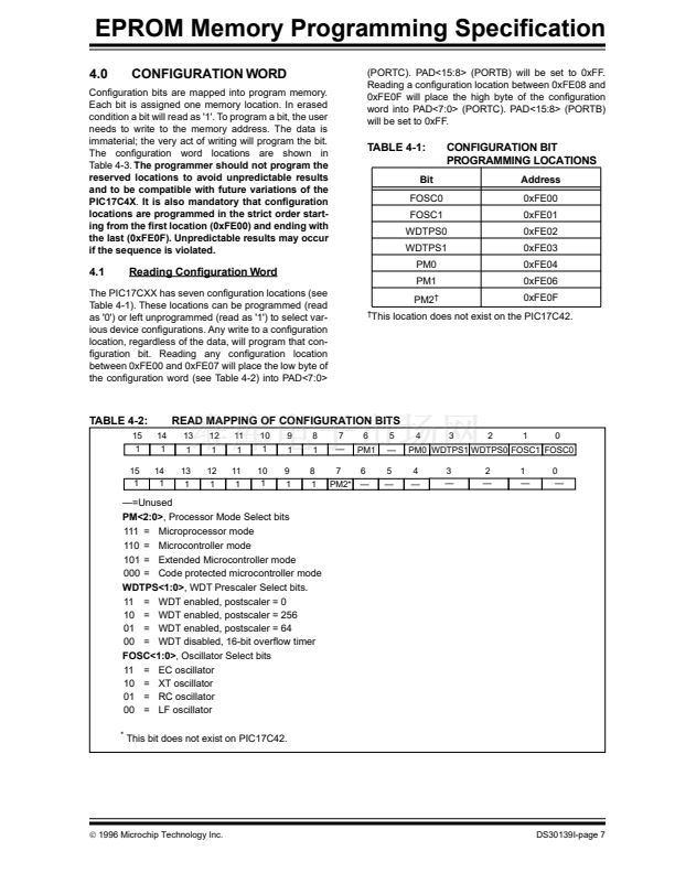
PAD <15:8>
PAD <7:0>
V
PP
V
DD
V
SS
Pin Type
I
I
I/O
I/O
P
P
P
Pin Description
Necessary in programming mode
Must be set to 鈥渉igh鈥?to enter programming mode
Address & data: high byte
Address & data: low byte
Programming Power
Power Supply
Ground
Legend: I = Input, O = Output, P = Power
1996 Microchip Technology Inc.
DS30139I-page 1
This document was created with FrameMaker 4 0 4


 1
1
 2
2
 3
3
 4
4
 5
5
 6
6
 7
7
 8
8
 9
9
 10
10
 11
11
 12
12
 13
13
 14
14
 15
15
 16
16
