STR-S6707
THRU
STR-S6709
OFF-LINE SWITCHING REGULATORS
鈥?WITH BIPOLAR SWITCHING TRANSISTOR
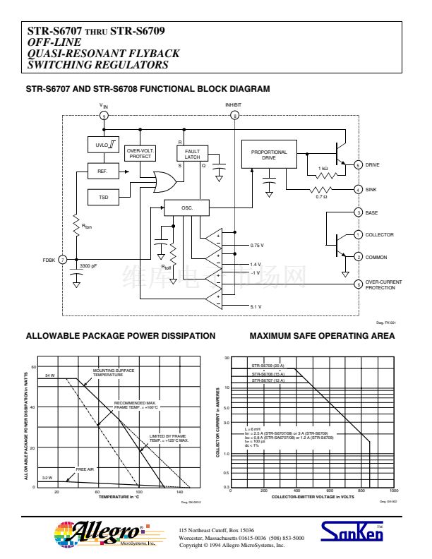
COLLECTOR
1
COMMON
2
FAULT
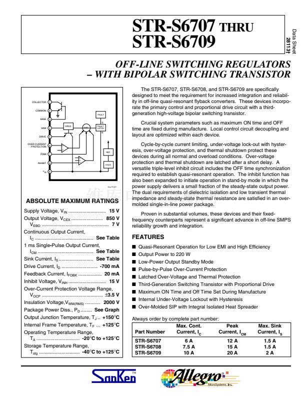
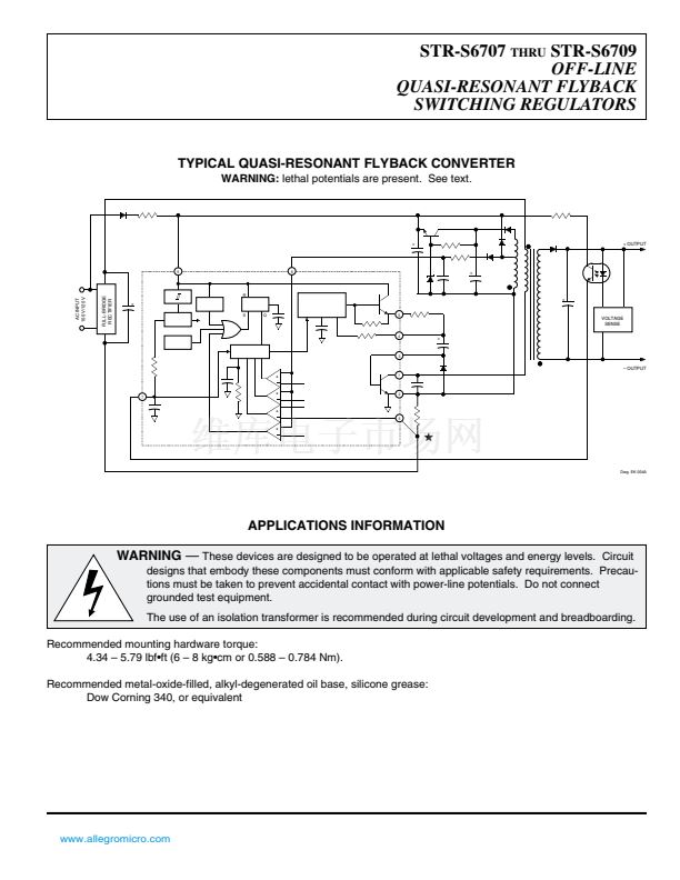
The STR-S6707, STR-S6708, and STR-S6709 are specifically
designed to meet the requirement for increased integration and reliabil-
ity in off-line quasi-resonant flyback converters. These devices incorpo-
rate the primary control and proportional drive circuit with a third-
generation high-voltage bipolar switching transistor.
Crucial system parameters such as maximum ON time and OFF
time are fixed during manufacture. Local control circuit decoupling and
layout are optimized within each device.
Cycle-by-cycle current limiting, under-voltage lock-out with hyster-
esis, over-voltage protection, and thermal shutdown protect these
devices during all normal and overload conditions. Over-voltage
protection and thermal shutdown are latched after a short delay. A
versatile triple-level inhibit circuit includes the OFF time synchronization
required to establish quasi-resonant operation. The inhibit function has
also been expanded to initiate operation in stand-by mode in which the
power supply delivers a small fraction of the steady-state output power.
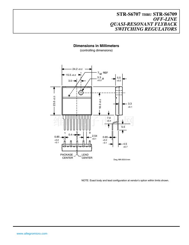
The dual requirements of dielectric isolation and low transient thermal
impedance and steady-state thermal resistance are satisfied in an over-
molded single-in-line power package.
Proven in substantial volumes, these devices and their fixed-
frequency counterparts represent a significant advance in off-line SMPS
reliability growth and integration.
Data Sheet
28113鈥?/div>
BASE
3
S
DRIVE
FAULT
LATCH
SINK
4
OSC.
R
DRIVE
OVER-CURRENT
PROTECTION
FDBK
5
6
+
REF.
7
INHIBIT
8
V IN
9
ABSOLUTE MAXIMUM RATINGS
Supply Voltage, V
IN
...........................
15 V
Output Voltage, V
CEX
.......................
850 V
V
EBO
................................................
7 V
Continuous Output Current,
I
C
..........................................
See Table
1 ms Single-Pulse Output Current,
I
CM
........................................
See Table
Sink Current, I
S
.........................
See Table
Drive Current, I
D
..........................
-700 mA
Feedback Current, I
FDBK
.................
20 mA
Inhibit Voltage, V
INH
...........................
15 V
Over-Current Protection Voltage Range,
V
OCP
............................................
卤
3.5 V
Insulation Voltage,V
WM(RMS)
...........
2000 V
Package Power Diss., P
D
........
See Graph
Output Junction Temperature, T
J
..
+150
掳
C
Internal Frame Temperature, T
F
...
+125
掳
C
Operating Temperature Range,
T
A
...............................
-20
掳
C to +125
掳
C
Storage Temperature Range,
T
stg
.............................
-40
掳
C to +125
掳
C
+
UVLO
Dwg. PK-001
FEATURES
I
I
I
I
I
I
I
I
I
Quasi-Resonant Operation for Low EMI and High Efficiency
Output Power to 220 W
Low-Power Output Standby Mode
Pulse-by-Pulse Over-Current Protection
Latched Over-Voltage and Thermal Protection
Third-Generation Switching Transistor with Proportional Drive
Maximum ON Time and Off Time Set During Manufacture
Internal Under-Voltage Lockout with Hysteresis
Over-Molded SIP with Integral Isolated Heat Spreader
Always order by complete part number:
Max. Cont.
Peak
Part Number
Current, I
C
Current, I
CM
STR-S6707
STR-S6708
STR-S6709
6A
7.5 A
10 A
12 A
15 A
20 A
Max. Sink
Current, I
S
1.5 A
1.5 A
2A
鈩?/div>
next


 1
1
 2
2
 3
3
 4
4
 5
5
 6
6
 7
7
 8
8
