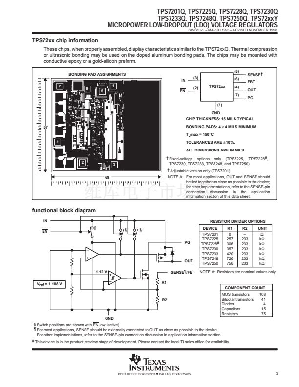
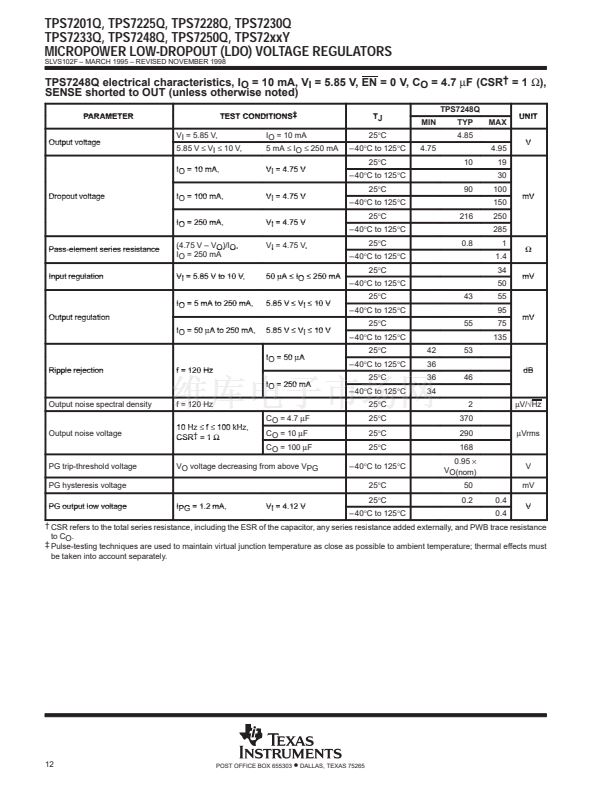
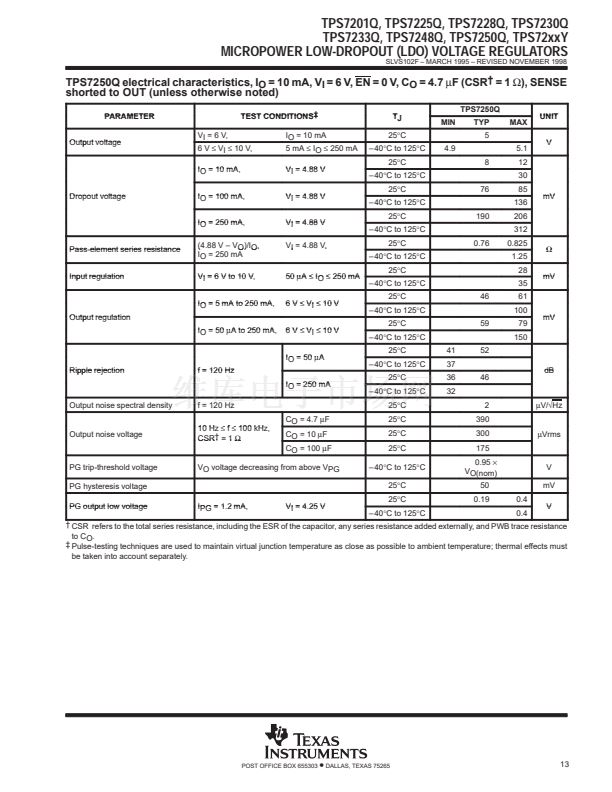
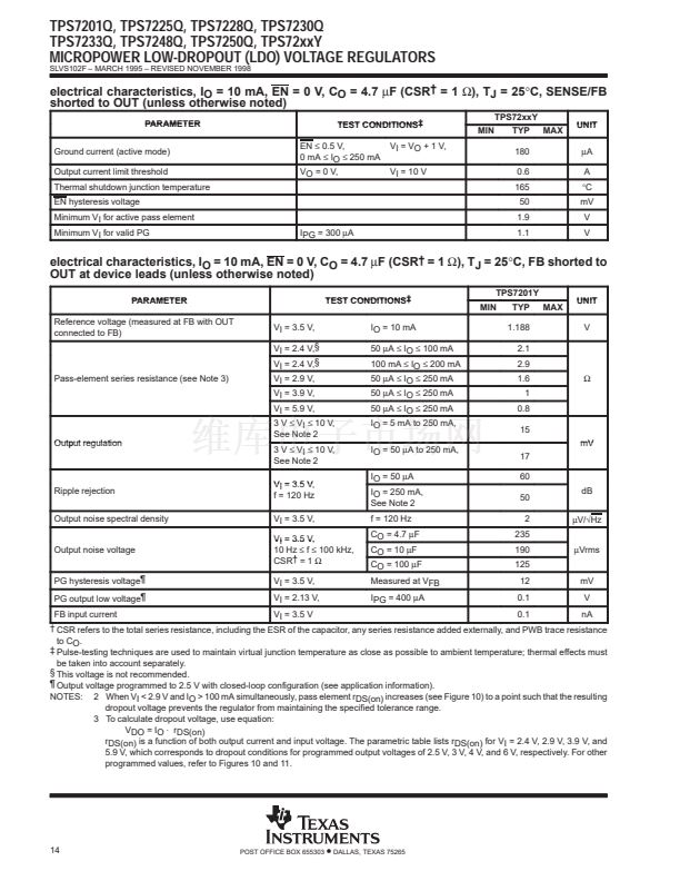
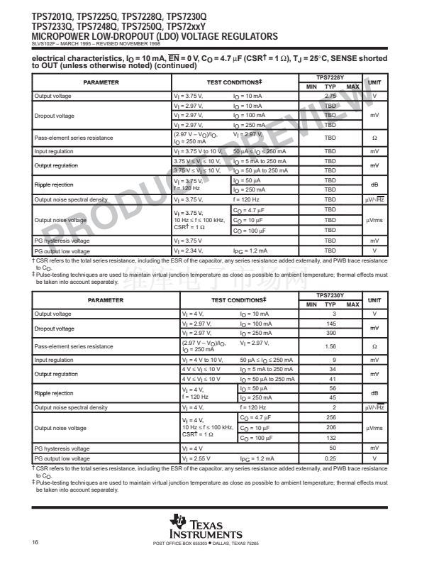
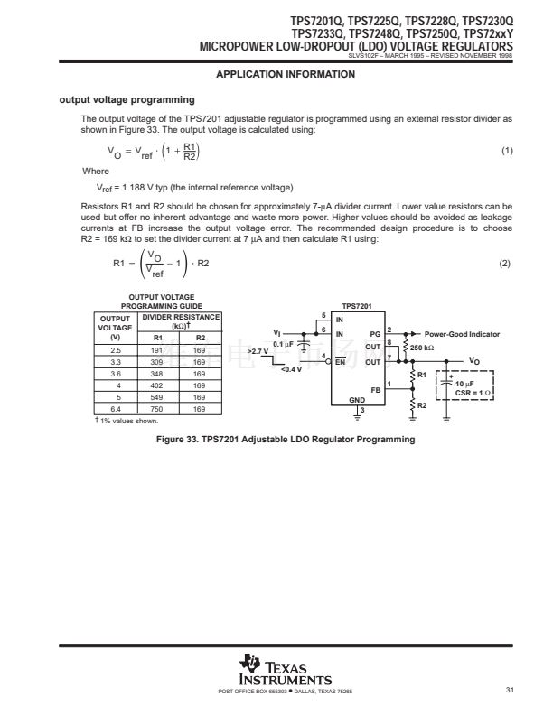
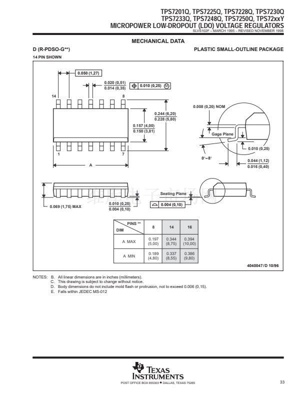
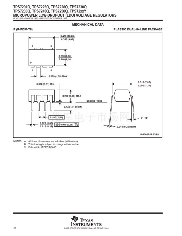
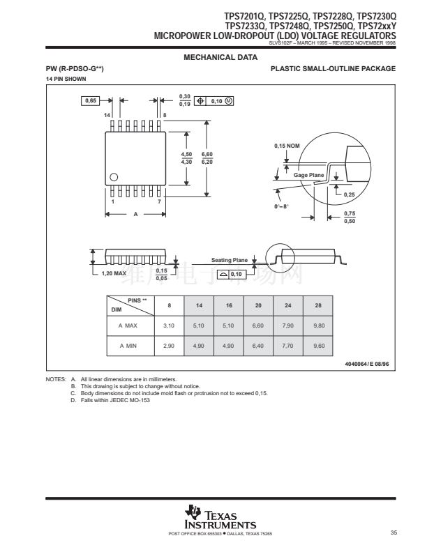
鈥?/div>
RESET/PG
GND
EN
1
2
3
4
8
7
6
5
OUT
OUT
IN
IN
鈥?SENSE 鈥?Fixed voltage options only
(TPS7225, TPS7228
搂
, TPS7230, TPS7233,
TPS7248, and TPS7250)
鈥?FB 鈥?Adjustable version only (TPS7201)
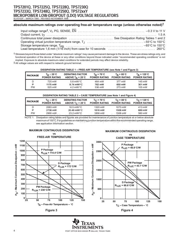
600
TA = 25掳C
500
TPS7225
400
TPS7230
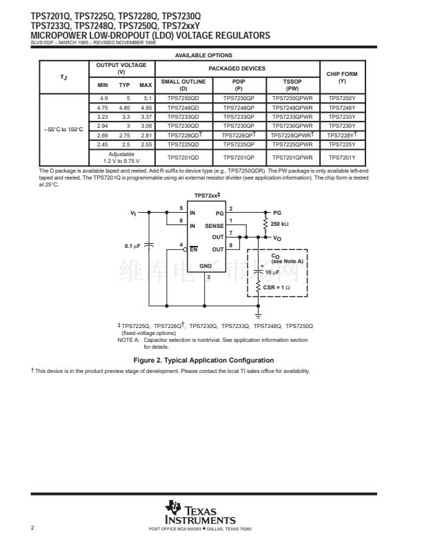
description
The TPS72xx family of low-dropout (LDO) voltage
regulators offers the benefits of low-dropout
voltage, micropower operation, and miniaturized
packaging. These regulators feature extremely
low dropout voltages and quiescent currents
compared to conventional LDO regulators.
Offered in small-outline integrated-circuit (SOIC)
packages and 8-terminal thin shrink small-outline
(TSSOP), the TPS72xx series devices are ideal
for cost-sensitive designs and for designs where
board space is at a premium.
300
TPS7233
200
TPS7248
100
TPS7250
0
A combination of new circuit design and process
0
50
100
150
200
250
innovation has enabled the usual pnp pass
IO 鈥?Output Current 鈥?mA
transistor to be replaced by a PMOS device.
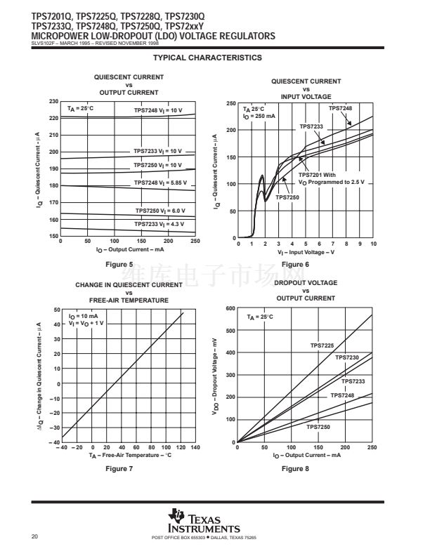
Figure 1. Typical Dropout Voltage Versus
Because the PMOS pass element behaves as a
Output Current
low-value resistor, the dropout voltage is very low
鈥?maximum of 85 mV at 100 mA of load current
(TPS7250) 鈥?and is directly proportional to the
load current (see Figure 1). Since the PMOS pass
element is a voltage-driven device, the quiescent current is very low (300
碌A
maximum) and is stable over the
entire range of output load current (0 mA to 250 mA). Intended for use in portable systems such as laptops and
cellular phones, the low-dropout voltage and micropower operation result in a significant increase in system
battery operating life.
The TPS72xx also features a logic-enabled sleep mode to shut down the regulator, reducing quiescent current
to 0.5
碌A
maximum at T
J
= 25掳C. Other features include a power-good function that reports low output voltage
and may be used to implement a power-on reset or a low-battery indicator.
The TPS72xx is offered in 2.5-V, 2.75-V
搂
, 3-V, 3.3-V, 4.85-V, and 5-V fixed-voltage versions and in an adjustable
version (programmable over the range of 1.2 V to 9.75 V). Output voltage tolerance is specified as a maximum
of 2% over line, load, and temperature ranges (3% for adjustable version).
搂 This device is in the product preview stage of development. Please contact the local TI sales office for availability.
Please be aware that an important notice concerning availability, standard warranty, and use in critical applications of
Texas Instruments semiconductor products and disclaimers thereto appears at the end of this data sheet.
This document contains information on products in more than one phase
of development. The status of each device is indicated on the page(s)
specifying its electrical characteristics.
Copyright
漏
1998, Texas Instruments Incorporated
POST OFFICE BOX 655303
鈥?/div>
DALLAS, TEXAS 75265
1


 1
1
 2
2
 3
3
 4
4
 5
5
 6
6
 7
7
 8
8
 9
9
 10
10
 11
11
 12
12
 13
13
 14
14
 15
15
 16
16
 17
17
 18
18
 19
19
 20
20
 21
21
 22
22
 23
23
 24
24
 25
25
 26
26
 27
27
 28
28
 29
29
 30
30
 31
31
 32
32
 33
33
 34
34
 35
35
 36
36
