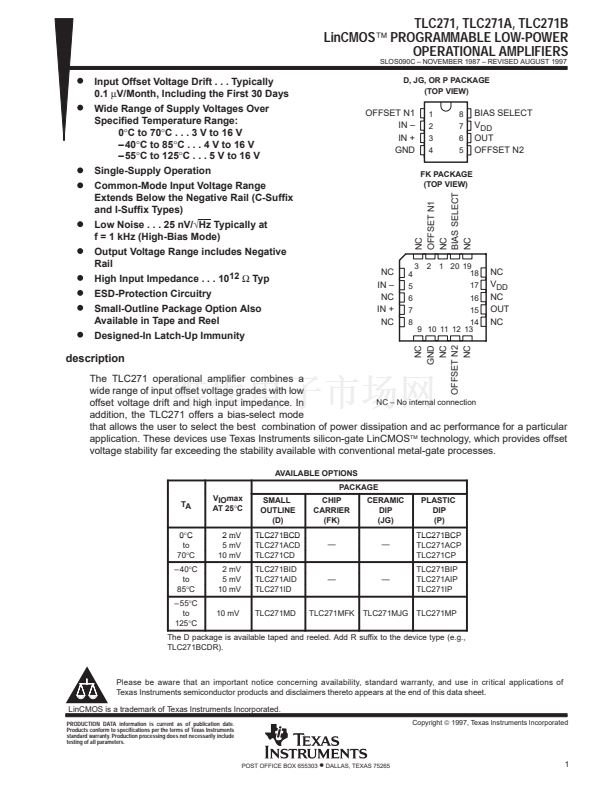
IN 鈥?/div>
IN +
GND
1
2
3
4
8
7
6
5
BIAS SELECT
V
DD
OUT
OFFSET N2
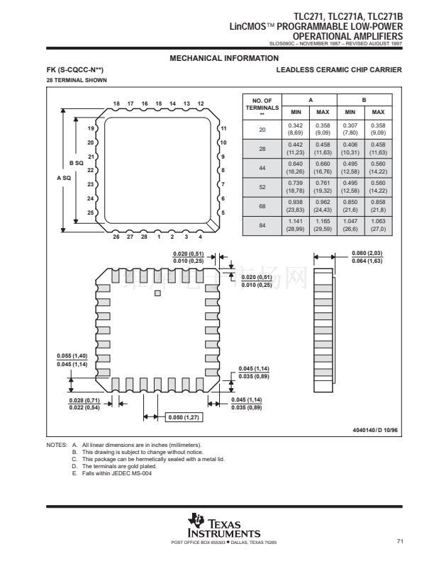
FK PACKAGE
(TOP VIEW)
description
The TLC271 operational amplifier combines a
wide range of input offset voltage grades with low
NC 鈥?No internal connection
offset voltage drift and high input impedance. In
addition, the TLC271 offers a bias-select mode
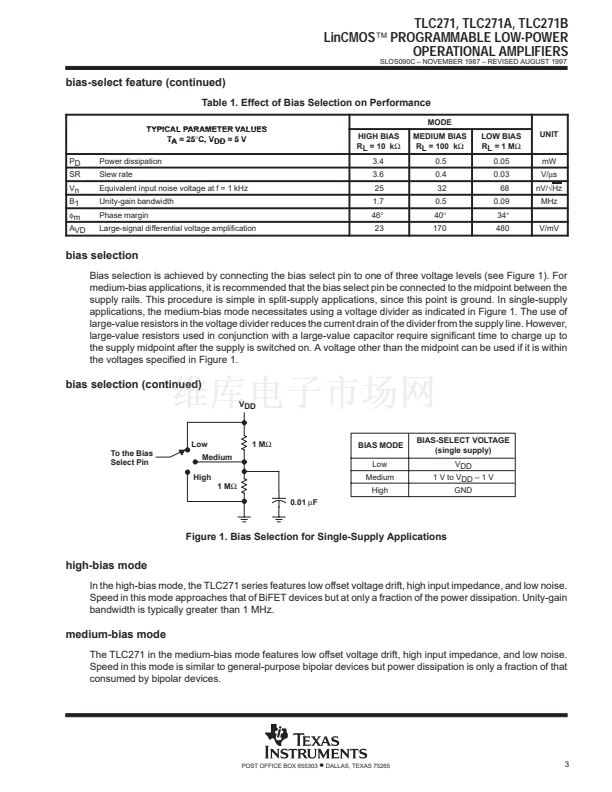
that allows the user to select the best combination of power dissipation and ac performance for a particular
application. These devices use Texas Instruments silicon-gate LinCMOS鈩?technology, which provides offset
voltage stability far exceeding the stability available with conventional metal-gate processes.
AVAILABLE OPTIONS
VIOmax
AT 25掳C
2 mV
5 mV
10 mV
2 mV
5 mV
10 mV
10 mV
SMALL
OUTLINE
(D)
TLC271BCD
TLC271ACD
TLC271CD
TLC271BID
TLC271AID
TLC271ID
TLC271MD
PLASTIC
DIP
(P)
TLC271BCP
TLC271ACP
TLC271CP
TLC271BIP
TLC271AIP
TLC271IP
TLC271MP
TA
0C
0掳C
to
70掳C
鈥?40 C
40掳C
to
85掳C
鈥?55掳C
to
125掳C
The D package is available taped and reeled. Add R suffix to the device type (e.g.,
TLC271BCDR).
Please be aware that an important notice concerning availability, standard warranty, and use in critical applications of
Texas Instruments semiconductor products and disclaimers thereto appears at the end of this data sheet.
LinCMOS is a trademark of Texas Instruments Incorporated.
PRODUCTION DATA information is current as of publication date.
Products conform to specifications per the terms of Texas Instruments
standard warranty. Production processing does not necessarily include
testing of all parameters.
POST OFFICE BOX 655303
鈥?/div>
DALLAS, TEXAS 75265
NC
GND
NC
OFFSET N2
NC
1


 1
1
 2
2
 3
3
 4
4
 5
5
 6
6
 7
7
 8
8
 9
9
 10
10
 11
11
 12
12
 13
13
 14
14
 15
15
 16
16
 17
17
 18
18
 19
19
 20
20
 21
21
 22
22
 23
23
 24
24
 25
25
 26
26
 27
27
 28
28
 29
29
 30
30
 31
31
 32
32
 33
33
 34
34
 35
35
 36
36
 37
37
 38
38
 39
39
 40
40
 41
41
 42
42
 43
43
 44
44
 45
45
 46
46
 47
47
 48
48
 49
49
 50
50
 51
51
 52
52
 53
53
 54
54
 55
55
 56
56
 57
57
 58
58
 59
59
 60
60
 61
61
 62
62
 63
63
 64
64
 65
65
 66
66
 67
67
 68
68
 69
69
 70
70
 71
71
 72
72
 73
73
 74
74
